Samsung SGH-i900 — Сервис-мануалы и схемы, разборка / сборка. Скачать бесплатно.

Samsung SGH-i900
— Руководство по обслуживанию. Скачать
![]()
Canon
i900D
i905D
PIXUS 900PD SERVICE MANUAL
Revision 0
QY8-1394-000
COPYRIGHT©2003 CANON INC. CANON PIXUS 900PD / i900D / i905D 092003 XX 0.00-0
Scope
This manual has been issued by Canon Inc., to provide the service technicians of this product with the information necessary for qualified persons to learn technical theory, installation, maintenance, and repair of products. The manual covers information applicable in all regions where the product is sold. For this reason, it may contain information that is not applicable to your region.
Revision
This manual could include technical inaccuracies or typographical errors due to improvements or changes made to the product. When changes are made to the contents of the manual, Canon will release technical information when necessary. When substantial changes are made to the contents of the manual, Canon will issue a revised edition.
The following do not apply if they do not conform to the laws and regulations of the region where the manual or product is used:
Trademarks
Product and brand names appearing in this manual are registered trademarks or trademarks of the respective holders.
Copyright
All rights reserved. No parts of this manual may be reproduced in any form or by any means or translated into another language without the written permission of Canon Inc., except in the case of internal business use.
Copyright 2003 by Canon Inc. CANON INC.
Inkjet Products Quality Assurance Div.
16-1, Shimonoge 3-chome, Takatsu-ku, Kawasaki, Kanagawa 213-8512, Japan
I.MANUAL OUTLINE
This manual consists of the following three parts to provide information necessary to service the i900D/i905D:
Part 1: Maintenance
Information on maintenance and troubleshooting of the i900D/i905D
Part 2: Technical Reference
New technology and technical information such as FAQ’s (Frequently Asked Questions) of the i900D/i905D
Part 3: Appendix
Block diagrams and pin layouts of the i900D/i905D
Reference:
This manual does not provide sufficient information of disassembly and reassembly procedures. Refer to the graphics in the separate Parts Catalog.
II.TABLE OF CONTENTS
Page Part 1: MAINTENANCE
1-1 1. MAINTENANCE
1.1Adjustment, Periodic Maintenance, Periodic Replacement Parts, and Replacement Consumables by Service Engineer
|
1-2 |
1.2 |
Customer Maintenance |
|
1-3 |
1.3 |
Product Life |
|
1.4 |
Special Tools |
|
|
1.5 |
Serial Number Location |
|
|
1-4 |
2. LIST OF ERROR DISPLAY / INDICATION |
|
|
2.1 |
Operator Call Errors (by LED Blinking in Orange) |
|
|
1-5 |
2.2 |
Service Call Errors |
|
1-6 |
2.3 |
Warnings |
|
1-7 |
2.4 |
Troubleshooting by Symptom |
|
1-8 |
3. REPAIR |
3.1Notes on Service Part Replacement (and Disassembling / Reassembling)
|
1-10 |
3.2 |
Special Notes on Repair Servicing |
|
|
1-12 |
3.3 |
Adjustment / Settings |
|
|
(1) |
Paper feed motor adjustment |
||
|
(2) |
Gear phase adjustment |
||
|
(3) |
Grease application |
||
|
(4) |
Waste ink counter setting |
||
|
(5) |
User mode |
||
|
(6) |
Service mode |
||
|
(7) |
Flash ROM upgrade |
||
|
1-20 |
3.4 |
Verification Items |
|
|
(1) |
Service test print |
||
|
(2) |
EEPROM information print |
1-22 4. PRINTER TRANSPORTATION METHOD
Part 2: TECHNICAL REFERENCE
|
2-1 |
1. |
NEW TECHNOLOGIES |
|
|
2-4 |
2. |
CLEANING MODE AND AMOUNT OF INK PURGED |
|
|
2-5 |
3. |
PRINT MODE |
|
|
2-7 |
4. |
PHOTO DIRECT PRINT FUNCTION |
|
|
4.1 |
Host PC Memory Card Access Function with the Memory Card Startup Utility |
||
|
2-8 |
4.2 |
Memory Card Direct Printing Function |
|
|
2-10 |
4.3 |
File Search |
|
|
2-11 |
4.4 |
File Sort |
|
|
4.5 |
Date Print |
||
|
2-12 |
4.6 |
Bubble Jet Direct Function |
|
|
2-14 |
4.7 |
PictBridge Function |
|
|
2-15 |
4.8 |
Exclusive Processes |
|
|
2-16 |
4.9 |
LCD Viewer |
|
|
2-17 |
4.10 |
Card Slot-related Operations and Display |
|
|
2-18 |
4.11 |
DPOF Settings in the Memory Card Direct Printing Function |
|
|
2-19 |
4.12 |
Print Layout (Details) |
|
|
2-21 |
4.13 |
Date Print Specifications |
|
|
2-22 |
4-14 |
Photo Number Printing Specifications |
|
|
2-23 |
5. |
FAQ (Specific Problems and Solutions) |
|
|
Part 3: |
APPENDIX |
||
|
3-1 |
1. |
BLOCK DIAGRAM |
|
|
3-2 |
2. |
CONNECTOR LOCATION AND PIN LAYOUT |
|
|
2.1 |
Logic Board Ass’y |
||
|
3-6 |
2.2 |
USB I/F Board (DCC Cover Unit) for Camera Direct Printing |
|
|
3-7 |
2.3 |
Operation Panel Board |
|
|
3-8 |
2.4 |
Memory Card Board |
|
|
3-12 |
2.5 |
Carriage Board (Print Head Connector) |
1.MAINTENANCE
1.1Adjustment, Periodic Maintenance, Periodic Replacement Parts, and Replacement Consumables by Service Engineer
(1)Adjustment
|
Adjustment |
Timing |
Purpose |
Tool |
Approx. |
|
|
time |
|||||
|
EEPROM |
At logic board ass’y replacement |
To initialize settings other than the |
None. |
1 min. |
|
|
initialization |
following: |
||||
|
(EEPROM settings) |
— USB serial number |
||||
|
— Destination setting |
|||||
|
(The language to be displayed on |
|||||
|
the LCD viewer is set to the default |
|||||
|
setting for each destination.) |
|||||
|
— Waste ink counter |
|||||
|
— Media sensor correction value |
|||||
|
— CD-R correction value |
|||||
|
Destination settings |
At logic board ass’y replacement |
To set the destination. |
None. |
1 min. |
|
|
(EEPROM settings) |
|||||
|
LCD viewer |
At logic board ass’y replacement |
To set the language to be displayed |
None. |
1 min. |
|
|
language settings |
on the LCD viewer. |
||||
|
Waste ink counter |
— At bottom case unit |
To reset the waste ink counter. |
None. |
1 min. |
|
|
resetting |
replacement |
||||
|
— At ink absorber (QC1-2232 / |
|||||
|
2233 / 2234 / 2235 / 2236) |
|||||
|
replacement |
|||||
|
Media sensor |
— At logic board ass’y |
To correct the media sensor. |
Calibration media |
2 min. |
|
|
correction*1 |
replacement |
kit (QY9-0064) |
|||
|
(EEPROM settings) |
— At sheet feeder unit |
||||
|
replacement |
|||||
|
CD-R sensor / |
— At logic board ass’y |
To correct the CD-R and automatic |
None. |
1 min. |
|
|
automatic print head |
replacement |
print head alignment sensor. |
(Correction |
||
|
alignment sensor |
— At carriage unit replacement |
performed |
|||
|
correction |
through service |
||||
|
(EEPROM settings) |
test print) |
||||
|
Print head alignment |
— At print head replacement |
To ensure accurate dot placement. |
— None. |
2 min. |
|
|
— At logic board ass’y |
(printer buttons) |
||||
|
replacement |
— Computer |
||||
|
(settings via the |
|||||
|
printer driver) |
|||||
|
Paper feed motor |
At paper feed motor unit |
To adjust the belt tension. (Position |
None. |
2 min. |
|
|
position |
replacement |
the paper feed motor so that the belt |
|||
|
adjustment*2 |
is stretched tight.) |
||||
|
Grease application |
— At carriage unit replacement |
— To maintain sliding properties of |
— FLOIL |
2 min. |
|
|
— At paper guide flapper ass’y |
the carriage, carriage shaft, paper |
KG-107A |
|||
|
(QL2-0341) replacement |
guide flapper, and lift cam shaft. |
(QY9-0057) |
|||
|
— At lift cam base’s (QL2-0340) |
— To protect the lift cam base gear. |
— MOLYKOTE |
|||
|
gear replacement |
PG641 |
||||
|
— At lift cam shaft unit |
(CK-0562) |
||||
|
(QM2-0593) replacement |
Note: DO NOT loosen the red screws on both sides of the main chassis, securing the carriage shaft positioning. *1: Media sensor correction
This operation adjusts the correction value of the media sensor, installed in the sheet feeder unit, to the EEPROM of the logic board ass’y. The adjustment is required when the sheet feeder unit or the logic board ass’y is replaced, and values are automatically determined via use of calibration media kit (QY9-0064: 10 sheet of reference plain paper and one sheet of reference white PET paper).
*2: Red screws of paper feed motor
The red screws securing the paper feed motor may be loosened only at replacement of the paper feed motor unit.
1 — 1
(2)Periodic maintenance
No periodic maintenance is necessary.
(3)Periodic replacement parts
There are no parts in this printer that require periodic replacement by a service engineer.
(4)Replacement consumables
There are no consumables that require replacement by a service engineer.
1.2Customer Maintenance
|
Adjustment |
Timing |
Purpose |
Tool |
Approx. |
|
|
time |
|||||
|
Print head alignment |
At print head |
To ensure accurate |
— Printer buttons |
3 min. |
|
|
replacement. |
dot placement. |
— Computer (settings |
|||
|
via the printer |
|||||
|
driver) |
|||||
|
Print head cleaning |
When print quality is |
To improve nozzle |
— Printer buttons |
30 sec. to |
|
|
not satisfying. |
conditions. |
— Computer (settings |
1 min. |
||
|
via the printer |
|||||
|
driver) |
|||||
|
Print head deep cleaning |
When print quality is |
To improve nozzle |
— Printer buttons |
1 to 1.5 |
|
|
not satisfying, and |
conditions. |
— Computer (settings |
min. |
||
|
not improved by |
via the printer |
||||
|
print head cleaning. |
driver) |
||||
|
Ink tank replacement |
When an ink tank |
2 min. |
|||
|
becomes empty. |
—— |
—— |
|||
|
(No ink error) |
|||||
|
Paper feed roller |
When paper does not |
To clean the paper |
Printer buttons |
2 min. |
|
|
cleaning |
feed properly. |
feed rollers. |
|||
|
CD-R print position |
At CD-R printing, |
To correct CD-R |
Computer (application |
5 min. |
|
|
adjustment |
when necessary |
print position |
software) |
||
|
LCD viewer contrast |
When adjusting the |
To adjust the |
Printer buttons |
1 min. |
|
|
adjustment |
contrast |
contrast |
1 — 2
1.3Product Life
(1)Printer
The value (i) or (ii), whichever comes first.
(i)5,000 pages of printing
|
— Black: |
1,500 pages |
(A4, |
1,500 character pattern) |
|
|
— Color: |
3,500 pages |
(A4, |
7.5% duty per color pattern: |
1,300 pages |
|
A4, 30% duty per color pattern: |
400 pages |
|||
|
Postcard, 30% duty per color pattern: |
800 pages |
|||
|
L-size, 30% duty per color pattern: |
1,000 pages) |
(ii)5 years of use
(2)Print head
5,000 pages (in the above print modes)
(3)Ink tank
|
BCI-6BK: |
540 pages (JEIDA standard pattern J1, plain paper, standard mode) |
|
520 pages (1,500 character pattern in black printing, plain paper, standard mode) |
|
|
540 pages (ISO JIS-SCID No. 5 pattern, plain paper, standard mode) |
|
|
BCI-6C: |
780 pages (ISO JIS-SCID No. 5 pattern, plain paper, standard mode) |
|
BCI-6M: |
580 pages (ISO JIS-SCID No. 5 pattern, plain paper, standard mode) |
|
BCI-6Y: |
360 pages (ISO JIS-SCID No. 5 pattern, plain paper, standard mode) |
|
BCI-6PC: |
410 pages (ISO JIS-SCID No. 5 pattern, plain paper, standard mode) |
|
BCI-6PM: |
260 pages (ISO JIS-SCID No. 5 pattern, plain paper, standard mode) |
1.4 Special Tools
|
Name |
Tool No. |
Purpose |
Remarks |
|
MOLYKOTE PG641 |
CK-0562-000 |
To be applied to the lift cam base’s |
In common with |
|
upper gear and the sliding portion |
conventional models |
||
|
of the lift cam shaft |
|||
|
FLOIL KG-107A |
QY9-0057-000 |
To be applied to the sliding |
In common with |
|
portions of the carriage, carriage |
conventional models |
||
|
shaft, and the paper guide flapper |
|||
|
GREASE EU1 |
QY9-0037-000 |
To be applied to the carriage shaft |
In common with |
|
bearing |
conventional models |
||
|
Calibration media kit |
QY9-0064-000 |
To correct the media sensor |
In common with |
|
conventional models |
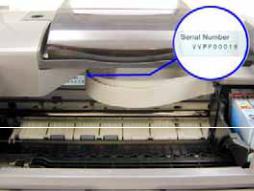
1.5Serial Number Location
Visible when the access cover is open.
1 — 3

2.LIST OF ERROR DISPLAY / INDICATION
Errors are indicated by the LED, and warnings are displayed on the monitor of the computer connected to the printer.
(1)Errors are indicated by the number of times the LED blinks.
(2)Errors are indicated in the LCD viewer on the operation panel.
(3)Warnings are displayed in the Status Monitor of the printer driver.
2.1Operator Call Errors (by LED Blinking in Orange)
|
LED |
Error |
Solution |
Remarks |
|
blinking |
|||
|
in orange |
|||
|
2 times |
No paper. (ASF) [1000] |
Set the paper in the ASF, and press the |
|
|
No CD-R tray. [1001]*1 |
Resume button. |
||
|
Set the CD-R tray, and press the Resume |
|||
|
button. |
|||
|
No paper in the photo paper tray. |
Set the paper in the photo paper tray, and |
||
|
[1004] |
press the Resume button. |
||
|
3 times |
Paper jam. [1300] |
Remove the jammed paper, and press the |
|
|
No ink. |
Resume button. |
||
|
4 times |
Replace the empty ink tank(s), or press the |
Pressing the Resume |
|
|
[1601/1602/1611/1612/1613/1634/ |
Resume button. |
button will exit the |
|
|
1635] |
error without ink tank |
||
|
replacement, however, |
|||
|
ink may run out during |
|||
|
printing. |
|||
|
5 times |
The print head is not installed |
Install the print head properly, and close the |
|
|
[1401], or it is not properly |
front cover. |
||
|
installed (EEPROM data of the |
Or, with the print head installed, turn the |
||
|
print head is faulty) [1403/1405]. |
printer off and on. |
||
|
6 times*1 |
No CD-R tray feeder (during |
Set the CD-R tray and tray feeder properly, |
|
|
CD-R printing). [1850/1855] |
and press the Resume button. |
||
|
Presence of the CD-R tray feeder |
Remove the CD-R tray feeder, and press the |
||
|
(during paper printing). |
Resume button. |
||
|
[1851/1856] |
|||
|
7 times*1 |
No CD-R or DVD-R. [1002] |
After setting a CD-R or DVD-R in the tray, |
|
|
set the tray in the tray feeder, and press the |
|||
|
Resume button. |
|||
|
8 times |
Warning: The waste ink absorber |
Pressing the Resume button will exit the |
The service call error, |
|
becomes almost full (approx. 95% |
error, and enable printing. |
indicating the waste |
|
|
of the maximum capacity). [1700] |
In repair servicing, replace the bottom case |
ink absorber is full, is |
|
|
unit (QM2-0663), or 5-item set of the ink |
likely to occur soon. |
||
|
absorbers |
|||
|
(QC1-2232/2233/2234/2235/2236). |
|||
|
9 times |
The connected digital camera or |
After removing the cable between the camera |
When connected to a |
|
digital video camera does not |
and the printer, press the Resume button, and |
Direct Print supported |
|
|
support Camera Direct Printing. |
re-connect the cable. |
camera, the green LED |
|
|
[2001] |
blinks 2 times. |
||
|
11 times |
Automatic print head alignment |
Press the Resume button, and after |
|
|
failure. [2500] |
confirming the following, perform print head |
||
|
alignment again: |
—Set an appropriate type and size of paper (plain paper, A4 or letter).
—Check that the nozzle check pattern is properly printed (all ink ejected, no faint printing)
—Check that the paper output slot is not exposed to light.
*1: Only for the model supporting CD-R printing (i905D only)
1 — 4
2.2Service Call Errors
—LED Blinking in Orange and Green Alternately, or Lit in Orange
—LCD viewer displaying error codes
|
LED |
|||
|
alternate blinking |
Error |
Solution |
|
|
in orange and |
(Replacement of listed parts, which are likely to be faulty) |
||
|
green |
|||
|
2 times |
Carriage error [5100] |
— Carriage unit (QM2-0662) |
|
|
— Timing slit strip film (QA4-1053) |
|||
|
— Logic board ass’y (QM2-0813/QM2-0814)*1 |
|||
|
— Carriage motor (QK1-0175) |
|||
|
3 times |
Paper feed error [6000] |
— Timing sensor unit (QM2-0596) |
|
|
— Timing slit disk film (QC1-2511) |
|||
|
— Feed roller ass’y (QF4-0155) |
|||
|
— Platen unit (QM2-0670/QM2-0675) |
|||
|
— Logic board ass’y (QM2-0813/QM2-0814)*1 |
|||
|
— Paper feed motor (QK1-0224) |
|||
|
4 times |
Purge unit error [5C00] |
— Purge unit (QM2-0656) |
|
|
— Logic board ass’y (QM2-0813/QM2-0814)*1 |
|||
|
6 times |
Internal temperature |
— Logic board ass’y (QM2-0813/QM2-0814)*1 |
|
|
error [5400] |
|||
|
7 times |
Waste ink absorber full |
— Ink absorbers (QC1-2232/2233/2234/2235/2236) |
|
|
[5B00] |
— Bottom case unit (QM2-0663)*3 |
||
|
8 times |
Print head temperature |
— Print head (QY6-0050) |
|
|
rise error [5200] |
— Logic board ass’y (QM2-0813/QM2-0814)*1 |
||
|
9 times |
EEPROM error [6800] |
— Logic board ass’y (QM2-0766/QM2-0767)*1 |
|
|
10 times*2 |
Carriage lift mechanism |
— Lift cam shaft unit (QM2-0593) |
|
|
error [5110] |
— Photo interrupter (WG8-5571) |
||
|
— Sheet feeder unit (QM2-0589) |
|||
|
— Logic board ass’y (QM2-0813/QM2-0814)*1 |
|||
|
12 times |
Media sensor error |
— Sheet feeder unit (QM2-0589) |
|
|
[8000] |
|||
|
13 times |
USB Host VBUS |
— Logic board ass’y (QM2-0813/QM2-0814)*1 |
|
|
overcurrent [9000] |
|||
|
15 times |
Other hardware error |
— Logic board ass’y (QM2-0813/QM2-0814)*1 |
|
|
[6500] |
|||
|
Continuous |
Flash ROM error |
— Logic board ass’y (QM2-0813/QM2-0814)*1 |
|
|
alternate blinking |
|||
|
Lights in orange |
RAM error |
— Logic board ass’y (QM2-0813/QM2-0814)*1 |
|
*1: Before replacement of the logic board ass’y, check the waste ink amount (by service test print or EEPROM information print). If the waste ink amount is 7% or more, also replace the bottom case unit (QM2-0586) or the 5-item set of the ink absorbers (QC1-2232/2233/2234/2235/2236) when replacing the logic board ass’y. See Section 3.3. Adjustment / Settings, (6) Service mode, for details.
*2: Only for models supporting CD-R printing (i905D only).
*3: Reset the waste ink counter when replacing the bottom case unit (QM2-0586). See Section 3.3. Adjustment / Settings, (6) Service mode, for details.
1 — 5

Printer (LCD viewer displaying)
Displayed warning
Low ink of 6BK, 6C, 6M, 6Y, 6PC or 6PM (at detection of no liquid ink remaining)
Print head temperature rise warning
Protection of excess rise of the print head temperature
Presence of the CD-R tray feeder*2
2.3Warnings
Remarks
If the print head temperature is high when the front cover is opened, the warning is displayed*1. When the print head temperature falls, the warning is released.
If the print head temperature exceeds the specified limit, a Wait is inserted during printing,
If the CD-R tray feeder is attached when the front cover is opened, the warning is displayed.*1 When the CD-R tray feeder is removed, and the front cover is closed, the warning is released.
*1: If the warning is displayed, the carriage does not move to the ink tank replacement position when the front cover is opened.
*2: Only for models supporting CD-R printing (i905D only).
1 — 6

2.4 Troubleshooting by Symptom
|
Symptom |
Solution |
Remarks |
|
|
Faulty |
The power does not turn on. |
Replace the |
|
|
The power turns off immediately |
— AC adapter, or |
||
|
*1 |
|||
|
after power-on. |
— logic board ass’y . |
||
|
operation |
|||
|
The print head is not recognized. |
Remove and re-install the print head, or replace the |
||
|
The print head does not move to |
— print head, or |
||
|
the home position. |
— logic board ass’y*1. |
||
|
A strange noise occurs. |
Remove foreign material, or attach a displaced part if |
||
|
any. |
|||
|
Printing stops mid-way. |
Replace the logic board ass’y*1. |
||
|
Paper |
Multiple sheets feed. |
Replace the |
|
|
— sheet feeder unit, or |
|||
|
— photo paper tray. |
|||
|
feed |
|||
|
Paper does not feed. |
Remove foreign material, or replace the |
||
|
problems |
— sheet feeder unit, or |
||
|
— photo paper tray. |
|||
|
Paper feeds at an angle. |
Remove foreign material, adjust the paper guide, or |
||
|
replace the |
|||
|
— sheet feeder unit, or |
|||
|
— photo paper tray. |
|||
|
Unsatisfactory |
No printing, or no color ejected. |
Replace the |
|
|
— ink tank, |
|||
|
— print head*2, |
|||
|
— logic board ass’y*1, or |
|||
|
Printing is faint, or white lines |
— purge unit. |
||
|
Remove and re-install the print head, or replace the |
|||
|
|
|||
|
appear on printouts even after |
— ink tank, |
||
|
print head cleaning. |
— print head*2, |
||
|
quality |
|||
|
Line(s) not included in the print |
— purge unit, or |
||
|
data appears on printouts. |
— logic board ass’y*1. |
||
|
Paper gets smeared. |
Feed several sheets of paper, or clean the paper path with |
||
|
cotton swab or cloth. |
|||
|
A part of a line is missing on |
Replace the |
||
|
printouts. |
— ink tank, or |
||
|
— print head*2. |
|||
|
Color hue is incorrect. |
Replace the |
||
|
— ink tank, or |
|||
|
— print head*2, or |
|||
|
correct the media sensor. |
|||
|
Printing is incorrect. |
Replace the logic board ass’y*1. |
||
|
No ejection of black ink. |
Replace the |
||
|
— ink tank, or |
|||
|
— print head*2. |
|||
|
Graphic or text is enlarged on |
When enlarged in the carriage movement direction, clean |
||
|
printouts. |
grease or oil off the timing slit strip film, or replace the |
||
|
— timing slit strip film, |
|||
|
— carriage unit, or |
|||
|
— logic board ass’y*1. |
|||
|
When enlarged in the paper feed direction, clean grease |
|||
|
or oil off the timing slit strip film, or replace the |
|||
|
— timing slit disk film, |
|||
|
— timing sensor unit, or |
|||
|
— logic board ass’y*1. |
*1: Before replacement of the logic board ass’y, check the waste ink amount (by service test print or EEPROM information print). If the waste ink amount is 7% or more, also replace the bottom case unit (QM2-0663) or the 5-item set of the ink absorbers (QC1-2232/2233/2234/2235/2236) when replacing the logic board ass’y. See Section 3.3. Adjustment / Settings, (6) Service mode, for details.
*2: Replace the print head only after the print head deep cleaning is performed 2 times, and the problem persists.
1 — 7

3.REPAIR
3.1Notes on Service Part Replacement (and Disassembling / Reassembling)
|
Service part |
Notes on replacement*1 |
Adjustment / settings |
Operation check |
||
|
After replacement: |
|||||
|
Logic board ass’y |
— Before removal of the |
— EEPROM |
|||
|
(QM2-0813/0814) |
logic board ass’y, remove |
1. |
Initialize the EEPROM. |
information print |
|
|
the power cord, and allow |
2. |
Reset the waste ink |
— Service test print |
||
|
for approx. 1 minute (for |
counter. |
— Printing via USB |
|||
|
discharge of capacitor’s |
3. |
Set the destination in |
connection |
||
|
accumulated charges), to |
the EEPROM. |
— Direct printing |
|||
|
prevent damages to the |
4. Set the LCD viewer’s |
from a digital |
|||
|
logic board ass’y. |
language. |
camera |
|||
|
— Before replacement, |
5. |
Correct the media |
|||
|
check the waste ink |
sensor. |
||||
|
amount (by service test |
6. |
Correct the CD-R and |
|||
|
print or EEPROM |
automatic print head |
||||
|
information print). If the |
alignment sensor. |
||||
|
waste ink amount is 7% |
For details of 1 to 5, see |
||||
|
or more, also replace the |
3.3. Adjustment / Settings, |
||||
|
bottom case unit or the |
(6) Service mode. |
||||
|
ink absorbers when |
|||||
|
replacing the logic board |
7. |
Perform the print head |
|||
|
ass’y. See 3.3. Adjustment |
alignment in the user |
||||
|
/ Settings, (6) Service |
mode. |
||||
|
mode, for details. |
|||||
|
Bottom case unit |
After replacement: |
— Service test print |
|||
|
(QM2-0663) |
1. |
Reset the waste ink |
|||
|
Ink absorber |
counter. See 3.3. |
||||
|
(QC1-2232/2233/ |
Adjustment / Settings, |
||||
|
2234/2235/2236) |
(6) Service mode. |
||||
|
Sheet feeder unit |
After replacement: |
— Service test print |
|||
|
(QM2-0589) |
1. |
Correct the media |
(Confirm media |
||
|
sensor. See 3.3. |
sensor correction.) |
||||
|
Adjustment / Settings, |
|||||
|
(6) Service mode. |
|||||
|
Carriage unit |
At replacement: |
— Service test print |
|||
|
(QM2-0662) |
1. |
Apply grease to the |
(Confirm CD-R |
||
|
sliding portions. See |
and automatic print |
||||
|
3.3. Adjustment / |
head alignment |
||||
|
Settings, (3) Grease |
sensor correction.) |
||||
|
application. |
|||||
|
After replacement: |
|||||
|
1. |
Correct the CD-R and |
||||
|
automatic print head |
|||||
|
alignment sensor. See |
|||||
|
3.3. Adjustment / |
|||||
|
Settings, (6) Service |
|||||
|
mode. |
|||||
|
2. |
Perform the print head |
||||
|
alignment in the user |
|||||
|
mode. |
|||||
|
Paper feed motor |
— The red screws securing |
At replacement: |
|||
|
(QK1-0224) |
the paper feed motor are |
1. |
Adjust the paper feed |
||
|
allowed to be loosened. |
motor. See 3.3. |
||||
|
(DO NOT loosen any |
Adjustment / Settings, |
||||
|
other red screws.) |
(1) Paper feed motor |
||||
|
adjustment. |
1 — 8

(Notes on Service Part Replacement and Disassembling / Reassembling — cont’d-)
|
Service part |
Notes on replacement*1 |
Adjustment / settings |
Operation check |
|
|
At replacement: |
||||
|
Lift cam shaft unit |
— Service test print |
|||
|
(QM2-0593) |
1. Apply grease to the |
|||
|
sliding portions. See |
||||
|
3.3. Adjustment / |
||||
|
Settings, (3) Grease |
||||
|
application. |
||||
|
2. Adjust the phase of the |
||||
|
lift shaft gear |
||||
|
(QC1-2297). See 3.3. |
||||
|
Adjustment / Settings, |
||||
|
(3) Grease application. |
||||
|
Timing slit strip film |
— Upon contact with the |
After replacement: |
— Service test print |
|
|
(QA4-1053) |
film, wipe the film with |
1. Perform the print head |
||
|
ethanol. |
alignment in the user |
|||
|
— Confirm no grease is on |
mode. |
|||
|
the film. (Wipe off any |
||||
|
Timing slit disk film |
||||
|
grease thoroughly with |
||||
|
(QC1-2511) |
||||
|
ethanol.) |
||||
|
— Do not bend the film. |
||||
|
Print head |
After replacement: |
— Service test print |
||
|
(QY6-0050) |
1. Perform the print head |
|||
|
alignment in the user |
||||
|
mode. |
||||
|
*1: General notes: |
—Make sure that the flexible cables and wires in the harness are in the proper position and connected correctly. See 3.2. Special Notes on Repair Servicing, (1) Flexible cable and harness wiring, connection, for details.
—Do not drop the ferrite core, which may cause damage.
—Protect electrical parts from damage due to static electricity.
—Before removing a unit, after removing the power cord, allow the printer to sit for approx. 1 minute (for capacitor discharging to protect the logic board ass’y from damages).
—Do not touch the timing slit strip film and timing slit disk film. No grease or abrasion is allowed.
—Protect the units from soiled with ink.
—Protect the housing from scratches.
—Exercise caution with the red screws, as follows:
i.The red screws of paper feed motor may be loosened only at replacement of the paper feed motor unit (DO NOT loosen them in other cases).
ii.DO NOT loosen the red screws on both sides of the main chassis, securing the carriage shaft positioning (they are not adjustable in servicing).
1 — 9

3.2Special Notes on Repair Servicing
(1)Flexible cable and harness wiring, connection
Use caution with the flexible cable and harness wiring. Improper wiring or connection may cause line breakage, possibly leading to ignition or emission of smoke.
(I)
(II)
(III)
(I)DSC direct connector harness wiring
DSC direct connector
Ground line
1 — 10
 Loading…
User Manual: Samsung SGH-i900 — Service manuals and Schematics, Disassembly / Assembly. Free.
Open the PDF directly: View PDF ![]() .
.
Page Count: 102 [warning: Documents this large are best viewed by clicking the View PDF Link!]

GSM TELEPHONE
SGH-i900
1. Safety Precautions
2. Specification
3. Product Function
4. Array course control
5. Exploded View and Parts list
6. MAIN Electrical Parts List
7. Disassembly and Assembly
Instructions
8. Block Diagrams
9. PCB Diagrams
10. Chart of Troubleshooting
11. Reference data
GSM TELEPHONE CONTENTS
This Service Manual is aproperty of Samsung Electronics Co.,Ltd.
Any unauthorized use of Manual can be punished under applicable
International and/or domestic law.
Samsung Electronics Co.,Ltd.
2008. 06. Rev.1.0
ⓒ
Country Web Site
North America service.samsungportal.com
Latin America latin.samsungportal.com
CIS cis.samsungportal.com
Europe europe.samsungportal.com
China china.samsungportal.com
Asia asia.samsungportal.com
Mideast &Africa mea.samsungportal.com
GSPN (Global Service Partner Network)

SAMSUNG Proprietary-Contents may change without notice
1. Safety Precautions
1-2
This Document can not be used without Samsung’s authorization
1-1. Repair Precaution
●Repair in Shield Box, during detailed tuning.
Take specially care of tuning or test,
because specipicty of cellular phone is sensitive for surrounding interference(RF noise).
●Be careful to use akind of magnetic object or tool,
because performance of parts is damaged by the influence of manetic force.
●Surely use astandard screwdriver when you disassemble this product,
otherwise screw will be worn away.
●Use athicken twisted wire when you measure level.
Athicken twisted wire has low resistance, therefore error of measurement is few.
●Repair after separate Test Pack and Set because for short danger (for example an
overcurrent and furious flames of parts etc) when you repair board in condition of
connecting Test Pack and tuning on.
●Take specially care of soldering, because Land of PCB is small and weak in heat.
●Surely tune on/off while using AC power plug, because arepair of battery charger is
dangerous when tuning ON/OFF PBA and Connector after disassembing charger.
●Don’t use as you pleases after change other material than replacement registered on SEC
System.
Otherwise engineer in charge isn’t charged with problem that you don’t keep this rules.

SAMSUNG Proprietary-Contents may change without notice
Safety Precautions
1-2
This Document can not be used without Samsung’s authorization
1-2. ESD(Electrostatically Sensitive Devices) Precaution
Several semiconductor may be damaged easilly by static electricity. Such parts are called by
ESD(Electrostatically Sensitive Devices), for example IC,BGA chip etc. Read Precaution below.
You can prevent from ESD damage by static electricity.
●Remove static electricity remained your body before you touch semiconductor or parts with
semiconductor. There are ways that you touch an earthed place or wear static electricity
prevention string on wrist.
●Use earthed soldering steel when you connect or disconnect ESD.
●Use soldering removing tool to break static electricity. ,otherwise ESD will be damaged by
static electricity.
●Don’t unpack until you set up ESD on product. Because most of ESD are packed by box
and aluminum plate to have conductive power,they are prevented from static electricity.
●You must maintain electric contact between ESD and place due to be set up until ESD is
connected completely to the proper place or acircuit board.

2. Specification
2-1
2-1. GSM General Specification
GSM850
Phase 1
EGSM 900
Phase 2
DCS1800
Phase 1 PCS1900 WCDMA2100
Freq.
Band[MHz]
Uplink/Downlink
824~849
869~894
880~915
925~960
1710~1785
1805~1880
1850~1910
1930~1990
1922~1977
2112~2167
ARFCN range 128~251 0~124 &
975~1023 512~885 512~810
UL:9612~9888
DL:10562~108
38
Tx/Rx spacing 45MHz 45MHz 95MHz 80MHz 190MHz
Mod. Bit rate/
Bit Period
270.833kbps
3.692us
270.833kbps
3.692us
270.833kbps
3.692us
270.833kbps
3.692us 3.84Mcps
Time Slot
Period/Frame
Period
576.9us
4.615ms
576.9us
4.615ms
576.9us
4.615ms
576.9us
4.615ms
FrameLength:
10ms
Slotlength:
0.667ms
Modulation 0.3GMSK 0.3GMSK 0.3GMSK 0.3GMSK QPSKHQPSK
MS Power 33dBm~5dBm 33dBm~5dBm 30dBm~0dBm 30dBm~0dB
m
24dBm~-
50dBm
Power Class 5pcl ~ 19pcl 5pcl ~19
pcl 0pcl ~15
pcl 0pcl ~15
pcl 3(max+24dBm)
Sensitivity -102dBm -102dBm -100dBm -100dBm -106.7dBm
TDMA Mux 8 8 8 8
Cell Radius 35Km 35Km 2Km 2Km 2Km
Specification
2-2
2-2. GSM Tx Power Class
TX Power
control
level
GSM850
533±2
dBm
631±2
dBm
729±2
dBm
827±2
dBm
925±2
dBm
10 23±2 dBm
11 21±2 dBm
12 19±2 dBm
13 17±2 dBm
14 15±2 dBm
15 13±2 dBm
16 11±3 dBm
17 9±3dBm
18 7±3 dBm
19 5±3 dBm
TX Power
control
level
EGSM900
533±2
dBm
631±2
dBm
729±2
dBm
827±2
dBm
925±2
dBm
10 23±2 dBm
11 21±2 dBm
12 19±2 dBm
13 17±2 dBm
14 15±2 dBm
15 13±2 dBm
16 11±3 dBm
17 9±3dBm
18 7±3 dBm
19 5±3 dBm
TX Power
control
level
DCS1800
030±3
dBm
128±3
dBm
226±3
dBm
324±3
dBm
422±3
dBm
520±3
dBm
618±3
dBm
716±3
dBm
814±3
dBm
912±4
dBm
10 10±4 dBm
11 8±4 dBm
12 6±4 dBm
13 4±4 dBm
14 2±5 dBm
15 0±5 dBm
TX Power
control
level
PCS1900
030±3
dBm
128±3
dBm
226±3
dBm
324±3
dBm
422±3
dBm
520±3
dBm
618±3
dBm
716±3
dBm
814±3
dBm
912±4
dBm
10 10±4 dBm
11 8±4 dBm
12 6±4 dBm
13 4±4 dBm
14 2±5 dBm
15 0±5 dBm

SAMSUNG Proprietary-Contents may change without notice
3. Product Function
3-1
This Document can not be used without Samsung’s authorization
Main Function
―Homescreen
―PIM —Contacts,Calendar,Tasks,Voice Note
―Messaging —SMS, MMS, Email,VoiceRecorder within MMS
―Windows Live! Portal
―Windows Update
―Email Setup Wizard
―Internet Explorer
―Multimedia capability -5Mega Pixel, Camcorder,Windows Media Player
―Zoomer
―Dialer
―Video Telephony
―Accessary Applications —Alarms, Calculator,NotePad,Task Manager,Smart Converter,World
Clock,Stopwatch,Smart Search
―Active Sync
―Bluetooth
―Document Viewer
―File Manager,My Item
―Java
―Pod Casting,RSS Reader
―Games
―MTV
―Postcard
―Google Map
―TV OUT
―Auto Brightness Control
―Acceleration Sensor
SAMSUNG Proprietary-Contents may change without notice
4. Array course control
4-1
This Document can not be used without Samsung’s authorization
4-1. Software Adjustments
There is 2set to download the binary image into your device.
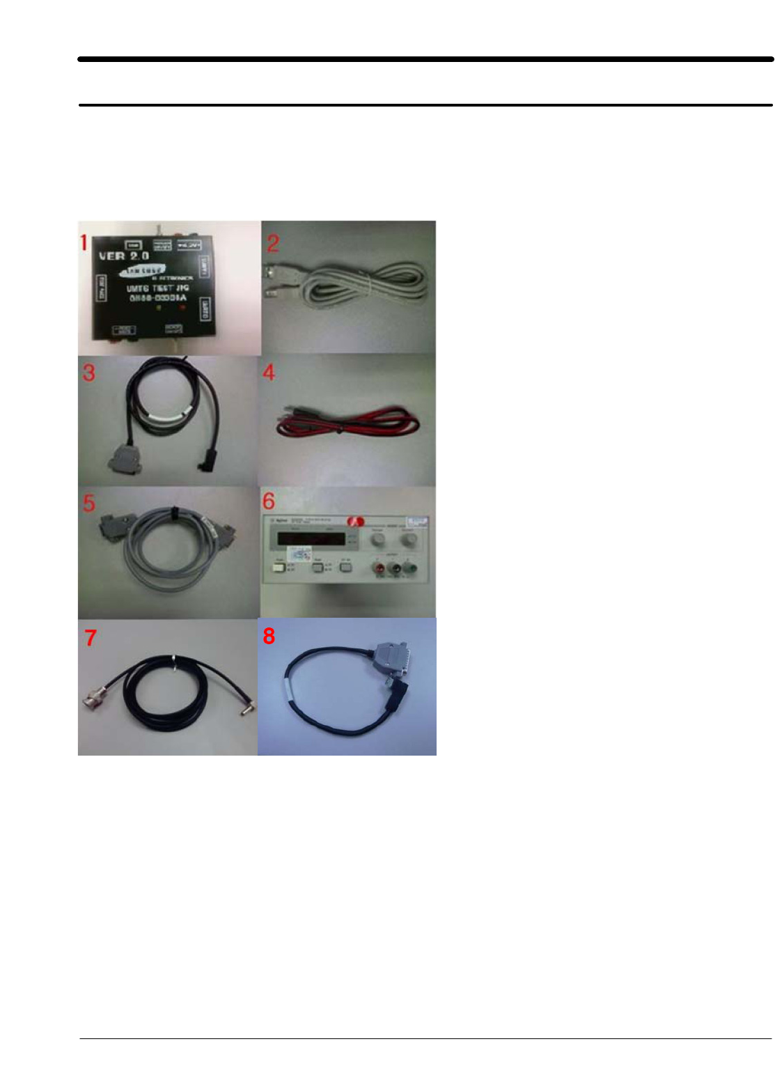
[First set]
1. JIG BOX (UMTS TEST JIG:GH80-03308A)
2. USB Cable :JIG to PC
3. Test Cable :JIG to SGH-i780 (GH39-00993A)
4. Power Cable :JIG to power supply
5. Serial Cable :SGH-i900 to PC
6. Power Supply
7. RF Cable (GH39-00599A): to Agilent 8960 or CMU200
8. Test Cable :JIG to SGH-i900 (GH39-00990A)
SAMSUNG Proprietary-Contents may change without notice
Array course control
4-2
This Document can not be used without Samsung’s authorization
[Second set]
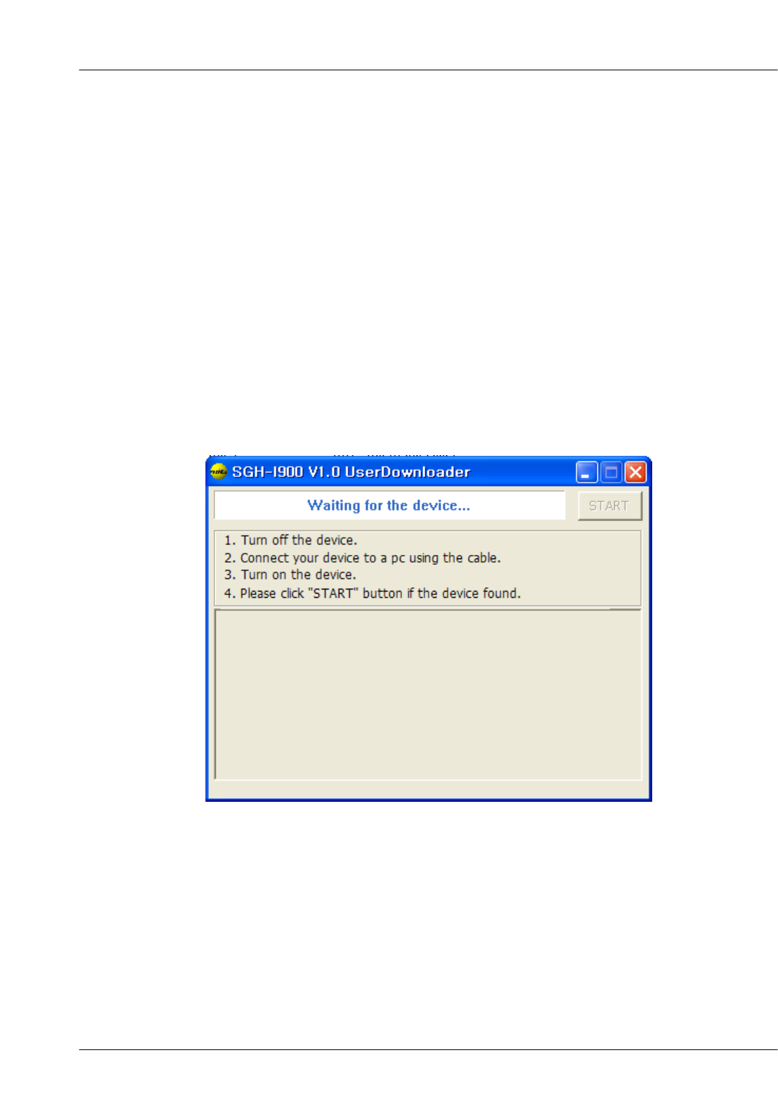
1. USB DATA Link Cable :GH39-00922A
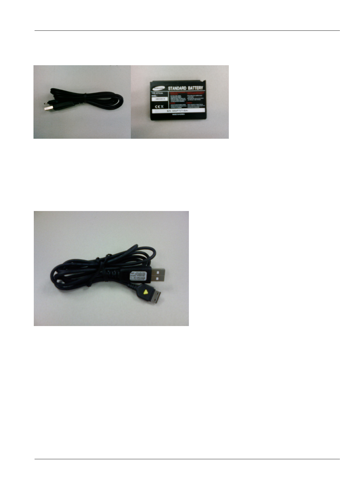
2. Battery :GH43-03110A
4-2. Software Download
1-1. Equipment for Software Download
1-2. Pre-requisite for Download
▶Downloader Program
—[Image Version].exe
▶USB Driver
—PDA :Samsung MITs USB Sync [Samsung MITs USB Sync.zip]
—Phone :Samsung CDMA Modem [Samsung CDMA Modem.zip]
▶SGH-i900 Mobile Device
▶Driver Installation
SAMSUNG Proprietary-Contents may change without notice
Array course control
4-3
This Document can not be used without Samsung’s authorization
2-1. Driver Installation (PDA)
▶Make sure that you install drivers.
▶If you installed the latest ActiveSync program, you don’t need to install the pda d
river. Please install the latest ActiveSync program.
2-2. Driver Installation (Phone)
When you download the phone image, you need the driver of Samsung CDMA Modem.
If you want to download the phone image, install the Samsung CDMA Modem driver.
)After you install the driver of Samsung CDMA Modem, please restart ahos
tcomputer.
3. Execute the Downloader Program. [Image Version.exe]
4. Turn off your device.
5. Connect your device to ahost computer by using USB DATA Link Ca
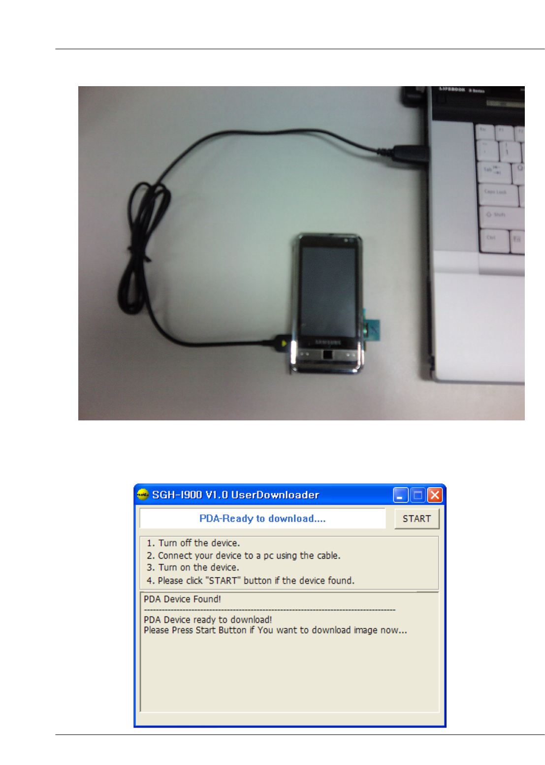
SAMSUNG Proprietary-Contents may change without notice
Array course control
4-4
This Document can not be used without Samsung’s authorization
ble.
6. Turn on your device and wait until ‘START’ button is activated.
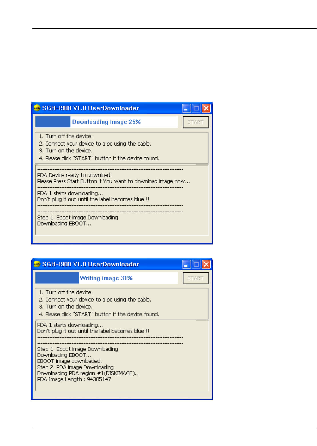
SAMSUNG Proprietary-Contents may change without notice
Array course control
4-5
This Document can not be used without Samsung’s authorization
)If ‘START’button is not activated, terminate the application and reconnect USB dat
alink cable and retry.
7. Please click “START”button.
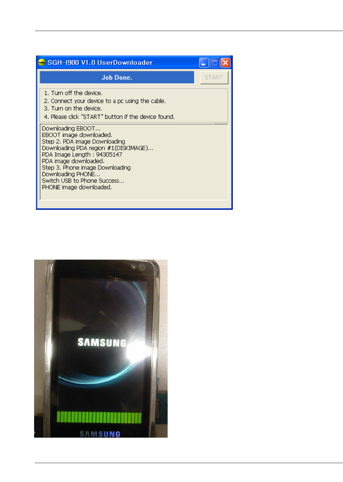
8. When the download is finished, the phone is rebooted automatically.
)Download Procedure
[Downloading EBOOT ]
[Downloading PDA ]
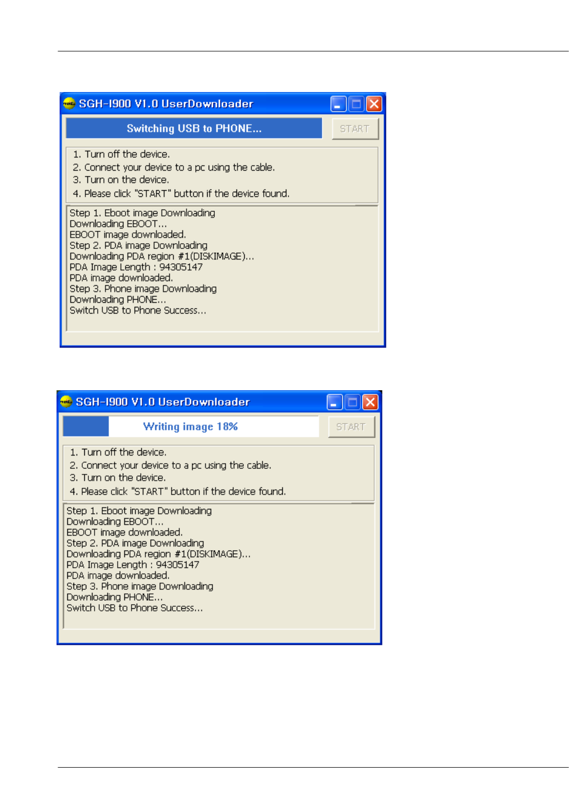
SAMSUNG Proprietary-Contents may change without notice
Array course control
4-6
This Document can not be used without Samsung’s authorization
[Changing USB PATH]
[Downloading PHONE ]
SAMSUNG Proprietary-Contents may change without notice
Array course control
4-7
This Document can not be used without Samsung’s authorization
[Job Done ]
)The Display of your Device
SAMSUNG Proprietary-Contents may change without notice
Array course control
4-8
This Document can not be used without Samsung’s authorization
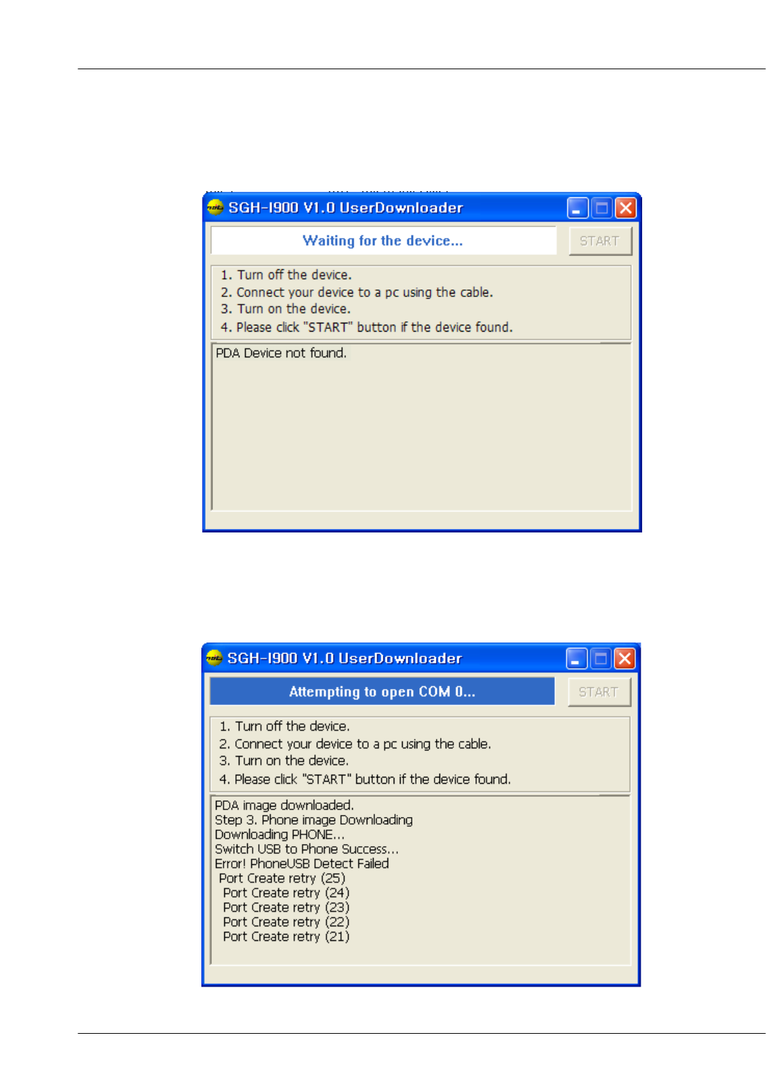
)Trouble Shooting
1. “PDA Device not found”message
)Make sure that your device is connected ahost computer by USB DATA Li
nk cable.
2. “Port Open Failed”message or application hang

SAMSUNG Proprietary-Contents may change without notice
Array course control
4-9
This Document can not be used without Samsung’s authorization
)After you install “phone USB driver (Samsung CDMA Modem)”at first time, you m
ay see “Port open failed…” message or application hang while downloading aphone
image. If so, terminate the application and then try the download again.
)If USB port is changed, at first time you may see “Port open failed…” message or
application hang. If so, terminate the application and then try the download again.
)If USB cable to the mobile device is not connected tightly, you may see “Port ope
nfailed…” message or application hang. If so, terminate the application and then try
the download again.
.
)If you always see “port open failed”message or application hang,
1. When failed application is activated, go to the device manager, remove the S
AMSUNG CDMA Modem and SAMSUNG USB Composite Device.
2. Rename C:WINDOWSsystem32driversModem.sys to other name. (ex. Mod
em-.sys)
3. Go to control panel->program add/remove, and then remove Samsung CDMA
ModemdriverorSamsungUSBdriver(MCCI)
4. Restart your PC.
5. Install attached SAMSUNG CDMA Modem_4.34
6. Try the download again.
3. “Write Failed”message
)If battery level is low, use charged battery and try again.
SAMSUNG Proprietary-Contents may change without notice
Array course control
4-10
This Document can not be used without Samsung’s authorization
—Reference —
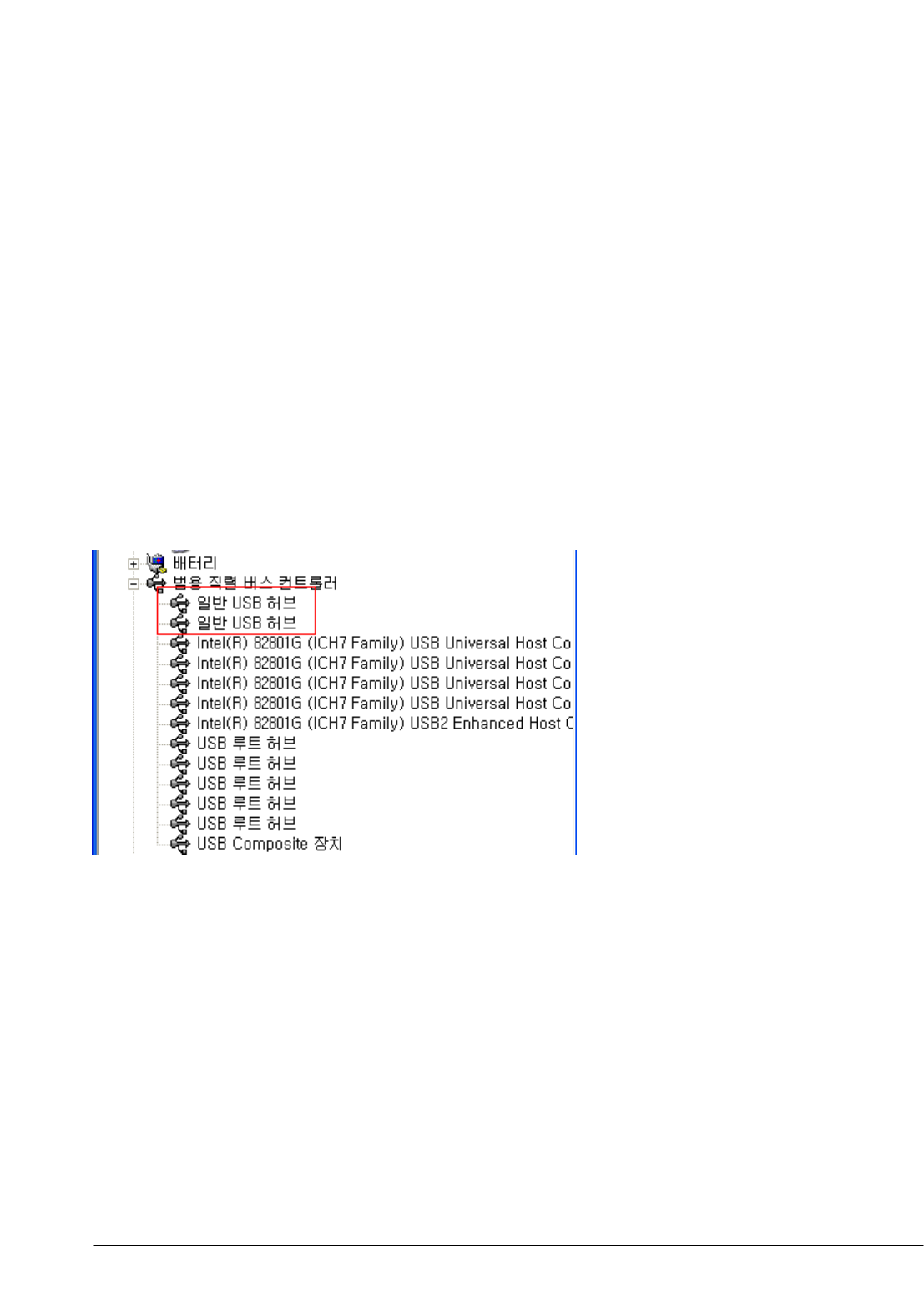
How to deal with the an error in the computer USB port of the computer.
Symptom: Device is not identified after connecting it.
Cause: The device is connected before the previous connection is complete. All devices should be
connected one by one. Otherwise, an error may occur in the computer USB port of the computer.
Solution:
Proceed with the following action in order only when the previous action does not work.
1) Unplug the USB port from the computer and plug it again.
2) Open the Device Manager and remove the USB hub and install it again.
3) Reboot the computer.
SAMSUNG Proprietary-Contents may change without notice
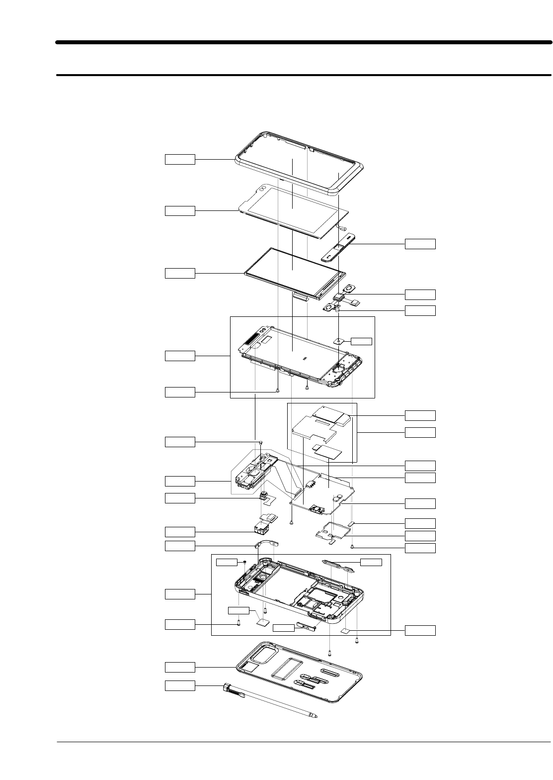
5. Exploded View and Parts List
5-1
This Document can not be used without Samsung’s authorization
5-1. Cellular phone Exploded View
QFR01
QME03
QLC01
QBR01
QCA07
QCR71
QCW02
QCA01
QCA02
QCK02
QRE01
QCR09
QBA00
QST01
QKP01
QJK01
QMI01
QCB01
QMP02
QAN05
QSH01
QCR71
QRF01
QVK01
QSH02
QMP01
QRF03
QCW01
QCR47 QVO01
QKP06

SAMSUNG Proprietary-Contents may change without notice
Exploded View and Parts List
5-2
This Document can not be used without Samsung’s authorization
Design LOC Discription SEC CODE
QAN05 ASSY RUBBER-INTENNA CONTACT GH98-08737A
QBA00 ASSY COVER-BATT GH98-09310A
QCA01 CAMERA MODULE-SGHI900 CIF GH59-05582A
QCA02 CAMERA MODULE-SGHI900 5M GH59-05583A
QCA07 KEY FPCB-SGHI900 CAMERA FPCB_C GH59-06056A
QCB01 CBF COAXIAL CABLE-SGHI900 MHF GH39-01069A
QCK02 PMO KEY-POWER FUNCTION GH72-47423A
QCR09 SCREW-MACHINE 6001-001670
QCR71 SCREW-MACHINE 6001-002095
QCR71 SCREW-MACHINE 6001-002095
QCW02 PMO DECO-WINDOW GH72-46895A
QFR01 NDC CASE-FRONT V2 GH71-08256A
QJK01 UNIT-SGHI900 OPTICAL JOYSTICK GH59-05596A
QKP01 ASSY KEYPAD-(XEF/XKA) GH98-07557A
QLC01 ELA UNIT-LCD UNIT ASSY(SGH_I90 GH96-03195A
QME03 UNIT-SGHI900 TOUCH WINDOW GH59-05586A
QMI01 MICROPHONE-ASSY-SGHI900 GH30-00473A
QMP01 PBA MAIN-SGHI900 GH92-04463A
QMP02 ASSY PBA MAIN-SGH_I900 16G GH92-04807A
QRF01 TAPE-RF SHEET GH74-37306A
QSH01 IPR SHIELD-CAN AGH70-03218A
QSH02 ASSY COVER-SHIELD CAN BGH98-09048A
QST01 ASSY ACCE-STYLUS PEN GH98-09044A
QVK01 KEY FPCB-SGHI900 VOLUME KEY GH59-05578A
QBR01 ASSY BRACKET GH98-07554A
QKP06 ASSY RUBBER-KEY DOM GH98-07631A
QRE01 ASSY CASE-REAR GH98-07553A
QCR47 SCREW-MACHINE 6001-001695
QCW01 ASSY COVER-CAMERA WINDOW GH98-07556A
QRF03 PMO COVER-EAR JACK V2 GH72-48359A
QVO01 ASSY KEY-CAM VOL GH98-08142A
5-2. Cellular phone Parts list

SAMSUNG Proprietary-Contents may change without notice
6. MAIN Electrical Parts List
6-1
This Document can not be used without Samsung’s authorization
SEC CODE Design LOC Discription
0403-001547 D301 DIODE-ZENER
0403-001547 D600 DIODE-ZENER
0406-001167 ZD403 DIODE-TVS
0406-001167 ZD404 DIODE-TVS
0406-001208 ZD402 DIODE-TVS
0406-001215 U502 DIODE-TVS
0406-001215 ZD400 DIODE-TVS
0406-001215 ZD401 DIODE-TVS
0406-001215 ZD405 DIODE-TVS
0406-001231 ZD500 DIODE-TVS
0406-001231 ZD501 DIODE-TVS
0406-001237 U208 DIODE-TVS
0406-001237 U308 DIODE-TVS
0406-001237 U312 DIODE-TVS
0406-001237 ZD406 DIODE-TVS
0406-001254 ZD300 DIODE-TVS
0406-001267 ZD201 DIODE-TVS
0407-001002 D300 DIODE-ARRAY
0407-001007 D302 DIODE-ARRAY
0501-002440 TR500 TR-SMALL SIGNAL
0501-002440 TR501 TR-SMALL SIGNAL
0501-002440 TR502 TR-SMALL SIGNAL
0504-000168 TR600 TR-DIGITAL
0801-002237 U205 IC-CMOS LOGIC
0801-002529 U206 IC-CMOS LOGIC
0801-002882 U311 IC-CMOS LOGIC
0801-003013 U207 IC-CMOS LOGIC
0801-003013 U503 IC-CMOS LOGIC
0801-003013 U504 IC-CMOS LOGIC
0801-003013 U515 IC-CMOS LOGIC
0801-003016 U201 IC-CMOS LOGIC
0801-003016 U516 IC-CMOS LOGIC
0801-003016 U602 IC-CMOS LOGIC
0801-003031 U204 IC-CMOS LOGIC
0801-003031 U600 IC-CMOS LOGIC
0801-003052 U203 IC-CMOS LOGIC
0801-003052 U307 IC-CMOS LOGIC
0801-003052 U608 IC-CMOS LOGIC
0801-003052 U609 IC-CMOS LOGIC
0801-003052 U610 IC-CMOS LOGIC
0902-002319 UCP600 IC-MICROPROCESSOR
1001-001231 U400 IC-ANALOG SWITCH

SAMSUNG Proprietary-Contents may change without notice
Main Electrical Parts List
6-2
This Document can not be used without Samsung’s authorization
SEC CODE Design LOC Discription
1001-001410 U300 IC-ANALOG SWITCH
1001-001436 U407 IC-ANALOG SWITCH
1001-001436 U408 IC-ANALOG SWITCH
1002-001410 U507 IC-D/A CONVERTER
1003-002047 U510 IC-MOTOR DRIVER
1006-001322 U505 IC-LINE TRANSCEIVER
1106-001564 UME201 IC-SRAM
1108-000127 UME200 IC-MCP
1108-000174 UCP600 IC-MCP
1201-002570 PAM100 IC-POWER AMP
1201-002581 F108 IC-RF AMP
1201-002597 U402 IC-AUDIO AMP
1201-002703 PAM101 IC-POWER AMP
1203-002832 U310 IC-VOL. DETECTOR
1203-003926 U305 IC-VOL. DETECTOR
1203-004291 U202 IC-MULTI REG.
1203-004319 U401 IC-MULTI REG.
1203-004435 U601 IC-MULTI REG.
1203-004548 U511 IC-DC/DC CONVERTER
1203-004571 U508 IC-MULTI REG.
1203-004763 U409 IC-VOL. DETECTOR
1203-004778 U301 IC-POWER SUPERVISOR
1203-004838 U303 IC-BATTERY
1203-004841 U605 IC-POWER SUPERVISOR
1203-004857 U506 IC-DC/DC CONVERTER
1203-005118 U514 IC-MULTI REG.
1203-005244 U101 IC-MULTI REG.
1203-005246 U500 IC-DC/DC CONVERTER
1203-005250 U512 IC-MULTI REG.
1203-005263 U509 IC-MULTI REG.
1204-002746 U405 IC-TUNER
1204-002749 UCD604 IC-PAL/NTSC ENCODER
1205-002686 U304 IC-SWITCH
1205-002720 UCD402 IC-CODEC
1205-002767 U302 IC-SWITCH
1205-003297 U100 IC-TRANSCEIVER
1205-003375 U603 IC-INTERFACE
1205-003498 UCP200 IC-MODEM
1209-001817 U607 IC-SENSOR
1404-001221 VR500 THERMISTOR-NTC
1405-001133 VR300 VARISTOR
2007-000070 L600 R-CHIP

SAMSUNG Proprietary-Contents may change without notice
Main Electrical Parts List
6-3
This Document can not be used without Samsung’s authorization
SEC CODE Design LOC Discription
2007-000148 R119 R-CHIP
2007-000162 R137 R-CHIP
2007-000164 R139 R-CHIP
2007-000170 R120 R-CHIP
2007-000171 R100 R-CHIP
2007-000171 R141 R-CHIP
2007-000171 R427 R-CHIP
2007-000171 R431 R-CHIP
2007-000171 R432 R-CHIP
2007-001285 R111 R-CHIP
2007-001285 R112 R-CHIP
2007-001290 R207 R-CHIP
2007-002965 R425 R-CHIP
2007-002965 R426 R-CHIP
2007-002965 R430 R-CHIP
2007-002965 R433 R-CHIP
2007-007468 R302 R-CHIP
2007-007468 R509 R-CHIP
2007-007517 R606 R-CHIP
2007-007741 R105 R-CHIP
2007-007741 R401 R-CHIP
2007-007741 R428 R-CHIP
2007-007741 R601 R-CHIP
2007-007741 R602 R-CHIP
2007-007766 R315 R-CHIP
2007-008015 R604 R-CHIP
2007-008040 R102 R-CHIP
2007-008044 R106 R-CHIP
2007-008045 R135 R-CHIP
2007-008046 R103 R-CHIP
2007-008046 R104 R-CHIP
2007-008049 R221 R-CHIP
2007-008052 R607 R-CHIP
2007-008052 R608 R-CHIP
2007-008055 R123 R-CHIP
2007-008055 R124 R-CHIP
2007-008055 R127 R-CHIP
2007-008055 R129 R-CHIP
2007-008055 R310 R-CHIP
2007-008055 R311 R-CHIP
2007-008055 R404 R-CHIP
2007-008055 R420 R-CHIP

SAMSUNG Proprietary-Contents may change without notice
Main Electrical Parts List
6-4
This Document can not be used without Samsung’s authorization
SEC CODE Design LOC Discription
2007-008055 R421 R-CHIP
2007-008055 R600 R-CHIP
2007-008263 R306 R-CHIP
2007-008263 R313 R-CHIP
2007-008419 R110 R-CHIP
2007-008419 R405 R-CHIP
2007-008419 R510 R-CHIP
2007-008419 R514 R-CHIP
2007-008419 R515 R-CHIP
2007-008438 R314 R-CHIP
2007-008456 R605 R-CHIP
2007-008483 R423 R-CHIP
2007-008486 R312 R-CHIP
2007-008516 R209 R-CHIP
2007-008516 R212 R-CHIP
2007-008516 R213 R-CHIP
2007-008516 R218 R-CHIP
2007-008516 R323 R-CHIP
2007-008516 R500 R-CHIP
2007-008516 R614 R-CHIP
2007-008542 R138 R-CHIP
2007-008542 R222 R-CHIP
2007-008542 R414 R-CHIP
2007-008542 R501 R-CHIP
2007-008542 R502 R-CHIP
2007-008542 R519 R-CHIP
2007-008542 R610 R-CHIP
2007-008542 R612 R-CHIP
2007-008542 R613 R-CHIP
2007-008542 R631 R-CHIP
2007-008548 R407 R-CHIP
2007-008548 R408 R-CHIP
2007-008548 R619 R-CHIP
2007-008548 R620 R-CHIP
2007-008588 R507 R-CHIP
2007-008588 R508 R-CHIP
2007-008588 R520 R-CHIP
2007-008588 R621 R-CHIP
2007-008588 R622 R-CHIP
2007-008686 R116 R-CHIP
2007-008708 R615 R-CHIP
2007-008739 R307 R-CHIP

SAMSUNG Proprietary-Contents may change without notice
Main Electrical Parts List
6-5
This Document can not be used without Samsung’s authorization
SEC CODE Design LOC Discription
2007-008798 R402 R-CHIP
2007-008798 U306 R-CHIP
2007-008806 R304 R-CHIP
2007-008806 R415 R-CHIP
2007-009084 R206 R-CHIP
2007-009084 R603 R-CHIP
2007-009108 R627 R-CHIP
2007-009155 R202 R-CHIP
2007-009155 R517 R-CHIP
2007-009157 R219 R-CHIP
2007-009157 R220 R-CHIP
2007-009157 R316 R-CHIP
2007-009157 R506 R-CHIP
2007-009157 R511 R-CHIP
2007-009157 R512 R-CHIP
2007-009170 R403 R-CHIP
2007-009170 R518 R-CHIP
2007-009170 R630 R-CHIP
2007-009171 R303 R-CHIP
2007-009171 R309 R-CHIP
2007-009171 R319 R-CHIP
2007-009171 R320 R-CHIP
2007-009171 R321 R-CHIP
2007-009171 R322 R-CHIP
2007-009212 R318 R-CHIP
2007-009212 R417 R-CHIP
2007-009212 R424 R-CHIP
2007-009323 R513 R-CHIP
2007-009354 R208 R-CHIP
2007-009361 R624 R-CHIP
2007-009361 R626 R-CHIP
2007-009402 R611 R-CHIP
2007-009408 R107 R-CHIP
2007-009408 R400 R-CHIP
2007-009408 R406 R-CHIP
2007-009420 R101 R-CHIP
2007-009801 R108 R-CHIP
2007-009801 R109 R-CHIP
2007-009801 R117 R-CHIP
2007-009801 R118 R-CHIP
2007-009801 R200 R-CHIP
2007-009801 R300 R-CHIP

SAMSUNG Proprietary-Contents may change without notice
Main Electrical Parts List
6-6
This Document can not be used without Samsung’s authorization
SEC CODE Design LOC Discription
2007-009801 R434 R-CHIP
2007-009801 R435 R-CHIP
2007-009801 R436 R-CHIP
2007-009954 R623 R-CHIP
2007-009969 R418 R-CHIP
2007-009969 R419 R-CHIP
2203-000233 C315 C-CER,CHIP
2203-000233 C319 C-CER,CHIP
2203-000233 C444 C-CER,CHIP
2203-000438 C170 C-CER,CHIP
2203-000438 C176 C-CER,CHIP
2203-000438 C219 C-CER,CHIP
2203-000438 C225 C-CER,CHIP
2203-000438 C611 C-CER,CHIP
2203-000438 C631 C-CER,CHIP
2203-000466 C1111 C-CER,CHIP
2203-000489 C237 C-CER,CHIP
2203-000725 C532 C-CER,CHIP
2203-000812 C103 C-CER,CHIP
2203-000812 C188 C-CER,CHIP
2203-002668 C174 C-CER,CHIP
2203-002668 C179 C-CER,CHIP
2203-002668 R122 C-CER,CHIP
2203-005234 C111 C-CER,CHIP
2203-005249 C416 C-CER,CHIP
2203-005249 C417 C-CER,CHIP
2203-005514 C435 C-CER,CHIP
2203-005514 C439 C-CER,CHIP
2203-005682 C1106 C-CER,CHIP
2203-005682 C117 C-CER,CHIP
2203-005682 C137 C-CER,CHIP
2203-005682 C138 C-CER,CHIP
2203-005682 C144 C-CER,CHIP
2203-005682 C156 C-CER,CHIP
2203-005682 C181 C-CER,CHIP
2203-005682 C244 C-CER,CHIP
2203-005682 C328 C-CER,CHIP
2203-005682 C329 C-CER,CHIP
2203-005682 C330 C-CER,CHIP
2203-005682 C409 C-CER,CHIP
2203-005682 C414 C-CER,CHIP
2203-005682 C418 C-CER,CHIP

SAMSUNG Proprietary-Contents may change without notice
Main Electrical Parts List
6-7
This Document can not be used without Samsung’s authorization
SEC CODE Design LOC Discription
2203-005682 C420 C-CER,CHIP
2203-005682 C423 C-CER,CHIP
2203-005682 C432 C-CER,CHIP
2203-005682 C456 C-CER,CHIP
2203-005682 C458 C-CER,CHIP
2203-005682 C462 C-CER,CHIP
2203-005719 C150 C-CER,CHIP
2203-005719 C442 C-CER,CHIP
2203-005719 C443 C-CER,CHIP
2203-005725 C1112 C-CER,CHIP
2203-005725 C1113 C-CER,CHIP
2203-005725 C1114 C-CER,CHIP
2203-005725 C115 C-CER,CHIP
2203-005725 C125 C-CER,CHIP
2203-005725 C132 C-CER,CHIP
2203-005725 C141 C-CER,CHIP
2203-005725 C146 C-CER,CHIP
2203-005725 C147 C-CER,CHIP
2203-005725 C160 C-CER,CHIP
2203-005725 C161 C-CER,CHIP
2203-005725 C164 C-CER,CHIP
2203-005725 C171 C-CER,CHIP
2203-005725 C177 C-CER,CHIP
2203-005727 C310 C-CER,CHIP
2203-005727 C317 C-CER,CHIP
2203-005727 C438 C-CER,CHIP
2203-005729 C434 C-CER,CHIP
2203-005729 C440 C-CER,CHIP
2203-005729 C642 C-CER,CHIP
2203-005729 C646 C-CER,CHIP
2203-005731 C175 C-CER,CHIP
2203-005732 C100 C-CER,CHIP
2203-005732 C101 C-CER,CHIP
2203-005736 C105 C-CER,CHIP
2203-005736 C107 C-CER,CHIP
2203-005736 C116 C-CER,CHIP
2203-005736 C118 C-CER,CHIP
2203-005736 C119 C-CER,CHIP
2203-005736 C120 C-CER,CHIP
2203-005736 C127 C-CER,CHIP
2203-005736 C128 C-CER,CHIP
2203-005736 C131 C-CER,CHIP

SAMSUNG Proprietary-Contents may change without notice
Main Electrical Parts List
6-8
This Document can not be used without Samsung’s authorization
SEC CODE Design LOC Discription
2203-005736 C143 C-CER,CHIP
2203-005736 C148 C-CER,CHIP
2203-005736 C153 C-CER,CHIP
2203-005736 C166 C-CER,CHIP
2203-005736 C172 C-CER,CHIP
2203-005736 C189 C-CER,CHIP
2203-005736 C323 C-CER,CHIP
2203-005740 C186 C-CER,CHIP
2203-005740 C187 C-CER,CHIP
2203-005740 C192 C-CER,CHIP
2203-005740 C193 C-CER,CHIP
2203-005740 C451 C-CER,CHIP
2203-005779 C413 C-CER,CHIP
2203-005779 C415 C-CER,CHIP
2203-005779 C419 C-CER,CHIP
2203-005779 C421 C-CER,CHIP
2203-005779 C426 C-CER,CHIP
2203-005779 C461 C-CER,CHIP
2203-005792 C152 C-CER,CHIP
2203-005792 C159 C-CER,CHIP
2203-005792 C180 C-CER,CHIP
2203-005806 C1104 C-CER,CHIP
2203-005806 C1105 C-CER,CHIP
2203-005806 C1107 C-CER,CHIP
2203-005806 C139 C-CER,CHIP
2203-005806 C452 C-CER,CHIP
2203-005806 C454 C-CER,CHIP
2203-006048 C245 C-CER,CHIP
2203-006053 C663 C-CER,CHIP
2203-006120 C182 C-CER,CHIP
2203-006120 C183 C-CER,CHIP
2203-006120 C184 C-CER,CHIP
2203-006123 L102 C-CER,CHIP
2203-006123 L103 C-CER,CHIP
2203-006123 L104 C-CER,CHIP
2203-006123 L105 C-CER,CHIP
2203-006194 C1109 C-CER,CHIP
2203-006194 C204 C-CER,CHIP
2203-006194 C206 C-CER,CHIP
2203-006194 C209 C-CER,CHIP
2203-006194 C220 C-CER,CHIP
2203-006194 C222 C-CER,CHIP

SAMSUNG Proprietary-Contents may change without notice
Main Electrical Parts List
6-9
This Document can not be used without Samsung’s authorization
SEC CODE Design LOC Discription
2203-006194 C224 C-CER,CHIP
2203-006194 C227 C-CER,CHIP
2203-006194 C402 C-CER,CHIP
2203-006194 C425 C-CER,CHIP
2203-006194 C428 C-CER,CHIP
2203-006194 C612 C-CER,CHIP
2203-006194 C615 C-CER,CHIP
2203-006194 C624 C-CER,CHIP
2203-006194 C630 C-CER,CHIP
2203-006208 C320 C-CER,CHIP
2203-006208 C408 C-CER,CHIP
2203-006208 C427 C-CER,CHIP
2203-006208 C535 C-CER,CHIP
2203-006305 C400 C-CER,CHIP
2203-006305 C407 C-CER,CHIP
2203-006307 C325 C-CER,CHIP
2203-006307 C326 C-CER,CHIP
2203-006324 C216 C-CER,CHIP
2203-006324 C324 C-CER,CHIP
2203-006348 C404 C-CER,CHIP
2203-006348 C453 C-CER,CHIP
2203-006379 C465 C-CER,CHIP
2203-006379 C466 C-CER,CHIP
2203-006379 C467 C-CER,CHIP
2203-006379 C468 C-CER,CHIP
2203-006399 C200 C-CER,CHIP
2203-006399 C205 C-CER,CHIP
2203-006399 C208 C-CER,CHIP
2203-006399 C211 C-CER,CHIP
2203-006399 C212 C-CER,CHIP
2203-006399 C213 C-CER,CHIP
2203-006399 C214 C-CER,CHIP
2203-006399 C239 C-CER,CHIP
2203-006399 C240 C-CER,CHIP
2203-006399 C311 C-CER,CHIP
2203-006399 C600 C-CER,CHIP
2203-006399 C601 C-CER,CHIP
2203-006423 C123 C-CER,CHIP
2203-006423 C124 C-CER,CHIP
2203-006423 C126 C-CER,CHIP
2203-006423 C129 C-CER,CHIP
2203-006423 C165 C-CER,CHIP

SAMSUNG Proprietary-Contents may change without notice
Main Electrical Parts List
6-10
This Document can not be used without Samsung’s authorization
SEC CODE Design LOC Discription
2203-006423 C201 C-CER,CHIP
2203-006423 C202 C-CER,CHIP
2203-006423 C207 C-CER,CHIP
2203-006423 C210 C-CER,CHIP
2203-006423 C215 C-CER,CHIP
2203-006423 C217 C-CER,CHIP
2203-006423 C218 C-CER,CHIP
2203-006423 C223 C-CER,CHIP
2203-006423 C228 C-CER,CHIP
2203-006423 C231 C-CER,CHIP
2203-006423 C234 C-CER,CHIP
2203-006423 C235 C-CER,CHIP
2203-006423 C238 C-CER,CHIP
2203-006423 C241 C-CER,CHIP
2203-006423 C242 C-CER,CHIP
2203-006423 C243 C-CER,CHIP
2203-006423 C305 C-CER,CHIP
2203-006423 C306 C-CER,CHIP
2203-006423 C308 C-CER,CHIP
2203-006423 C327 C-CER,CHIP
2203-006423 C331 C-CER,CHIP
2203-006423 C401 C-CER,CHIP
2203-006423 C403 C-CER,CHIP
2203-006423 C405 C-CER,CHIP
2203-006423 C406 C-CER,CHIP
2203-006423 C424 C-CER,CHIP
2203-006423 C433 C-CER,CHIP
2203-006423 C469 C-CER,CHIP
2203-006423 C524 C-CER,CHIP
2203-006423 C634 C-CER,CHIP
2203-006423 C641 C-CER,CHIP
2203-006423 C647 C-CER,CHIP
2203-006423 C648 C-CER,CHIP
2203-006423 C649 C-CER,CHIP
2203-006423 C650 C-CER,CHIP
2203-006423 C658 C-CER,CHIP
2203-006423 C659 C-CER,CHIP
2203-006423 C660 C-CER,CHIP
2203-006423 C661 C-CER,CHIP
2203-006423 C662 C-CER,CHIP
2203-006423 C670 C-CER,CHIP
2203-006423 C672 C-CER,CHIP

SAMSUNG Proprietary-Contents may change without notice
Main Electrical Parts List
6-11
This Document can not be used without Samsung’s authorization
SEC CODE Design LOC Discription
2203-006423 U200 C-CER,CHIP
2203-006423 U309 C-CER,CHIP
2203-006462 C246 C-CER,CHIP
2203-006466 C671 C-CER,CHIP
2203-006474 C314 C-CER,CHIP
2203-006474 C667 C-CER,CHIP
2203-006474 C668 C-CER,CHIP
2203-006474 C674 C-CER,CHIP
2203-006474 C677 C-CER,CHIP
2203-006556 C114 C-CER,CHIP
2203-006556 C203 C-CER,CHIP
2203-006562 C195 C-CER,CHIP
2203-006562 C198 C-CER,CHIP
2203-006562 C226 C-CER,CHIP
2203-006562 C229 C-CER,CHIP
2203-006562 C232 C-CER,CHIP
2203-006562 C233 C-CER,CHIP
2203-006562 C236 C-CER,CHIP
2203-006562 C307 C-CER,CHIP
2203-006562 C445 C-CER,CHIP
2203-006562 C446 C-CER,CHIP
2203-006562 C450 C-CER,CHIP
2203-006562 C455 C-CER,CHIP
2203-006562 C457 C-CER,CHIP
2203-006562 C459 C-CER,CHIP
2203-006562 C503 C-CER,CHIP
2203-006562 C504 C-CER,CHIP
2203-006562 C505 C-CER,CHIP
2203-006562 C513 C-CER,CHIP
2203-006562 C519 C-CER,CHIP
2203-006562 C541 C-CER,CHIP
2203-006562 C542 C-CER,CHIP
2203-006562 C602 C-CER,CHIP
2203-006562 C603 C-CER,CHIP
2203-006562 C604 C-CER,CHIP
2203-006562 C605 C-CER,CHIP
2203-006562 C606 C-CER,CHIP
2203-006562 C608 C-CER,CHIP
2203-006562 C610 C-CER,CHIP
2203-006562 C614 C-CER,CHIP
2203-006562 C617 C-CER,CHIP
2203-006562 C619 C-CER,CHIP

SAMSUNG Proprietary-Contents may change without notice
Main Electrical Parts List
6-12
This Document can not be used without Samsung’s authorization
SEC CODE Design LOC Discription
2203-006562 C620 C-CER,CHIP
2203-006562 C622 C-CER,CHIP
2203-006562 C625 C-CER,CHIP
2203-006562 C627 C-CER,CHIP
2203-006562 C628 C-CER,CHIP
2203-006562 C638 C-CER,CHIP
2203-006562 C643 C-CER,CHIP
2203-006562 C654 C-CER,CHIP
2203-006585 C447 C-CER,CHIP
2203-006585 C448 C-CER,CHIP
2203-006642 C169 C-CER,CHIP
2203-006648 C678 C-CER,CHIP
2203-006707 C157 C-CER,CHIP
2203-006824 C162 C-CER,CHIP
2203-006824 C163 C-CER,CHIP
2203-006824 C221 C-CER,CHIP
2203-006824 C301 C-CER,CHIP
2203-006824 C302 C-CER,CHIP
2203-006824 C422 C-CER,CHIP
2203-006824 C500 C-CER,CHIP
2203-006824 C655 C-CER,CHIP
2203-006824 C666 C-CER,CHIP
2203-006824 C669 C-CER,CHIP
2203-006824 C673 C-CER,CHIP
2203-006824 C675 C-CER,CHIP
2203-006838 C1101 C-CER,CHIP
2203-006838 C1102 C-CER,CHIP
2203-006838 C199 C-CER,CHIP
2203-006838 C300 C-CER,CHIP
2203-006838 C303 C-CER,CHIP
2203-006838 C304 C-CER,CHIP
2203-006838 C316 C-CER,CHIP
2203-006838 C322 C-CER,CHIP
2203-006838 C410 C-CER,CHIP
2203-006838 C411 C-CER,CHIP
2203-006838 C412 C-CER,CHIP
2203-006838 C523 C-CER,CHIP
2203-006838 C525 C-CER,CHIP
2203-006838 C530 C-CER,CHIP
2203-006838 C533 C-CER,CHIP
2203-006838 C534 C-CER,CHIP
2203-006838 C537 C-CER,CHIP

SAMSUNG Proprietary-Contents may change without notice
Main Electrical Parts List
6-13
This Document can not be used without Samsung’s authorization
SEC CODE Design LOC Discription
2203-006838 C538 C-CER,CHIP
2203-006838 C540 C-CER,CHIP
2203-006838 C543 C-CER,CHIP
2203-006838 C544 C-CER,CHIP
2203-006838 C546 C-CER,CHIP
2203-006838 C547 C-CER,CHIP
2203-006838 C549 C-CER,CHIP
2203-006838 C635 C-CER,CHIP
2203-006838 C636 C-CER,CHIP
2203-006838 C637 C-CER,CHIP
2203-006839 C102 C-CER,CHIP
2203-006839 C106 C-CER,CHIP
2203-006839 C108 C-CER,CHIP
2203-006839 C1108 C-CER,CHIP
2203-006839 C113 C-CER,CHIP
2203-006839 C133 C-CER,CHIP
2203-006839 C140 C-CER,CHIP
2203-006839 C142 C-CER,CHIP
2203-006839 C149 C-CER,CHIP
2203-006839 C154 C-CER,CHIP
2203-006839 C173 C-CER,CHIP
2203-006839 C178 C-CER,CHIP
2203-006839 C185 C-CER,CHIP
2203-006839 C449 C-CER,CHIP
2203-006839 C517 C-CER,CHIP
2203-006839 C518 C-CER,CHIP
2203-006839 C521 C-CER,CHIP
2203-006839 C527 C-CER,CHIP
2203-006839 C548 C-CER,CHIP
2203-006839 C607 C-CER,CHIP
2203-006839 C609 C-CER,CHIP
2203-006839 C613 C-CER,CHIP
2203-006839 C616 C-CER,CHIP
2203-006839 C618 C-CER,CHIP
2203-006839 C621 C-CER,CHIP
2203-006839 C623 C-CER,CHIP
2203-006839 C626 C-CER,CHIP
2203-006839 C629 C-CER,CHIP
2203-006839 C632 C-CER,CHIP
2203-006839 C639 C-CER,CHIP
2203-006839 C653 C-CER,CHIP
2203-006839 C657 C-CER,CHIP

SAMSUNG Proprietary-Contents may change without notice
Main Electrical Parts List
6-14
This Document can not be used without Samsung’s authorization
SEC CODE Design LOC Discription
2203-006839 C679 C-CER,CHIP
2203-006839 C680 C-CER,CHIP
2203-006839 C681 C-CER,CHIP
2203-006839 C682 C-CER,CHIP
2203-006841 C309 C-CER,CHIP
2203-006872 C194 C-CER,CHIP
2203-006872 C196 C-CER,CHIP
2203-006872 C197 C-CER,CHIP
2203-006872 C318 C-CER,CHIP
2203-006872 C321 C-CER,CHIP
2203-006872 C508 C-CER,CHIP
2203-006872 C509 C-CER,CHIP
2203-006872 C510 C-CER,CHIP
2203-006872 C511 C-CER,CHIP
2203-006872 C512 C-CER,CHIP
2203-006872 C656 C-CER,CHIP
2203-006872 C664 C-CER,CHIP
2203-006872 C665 C-CER,CHIP
2203-006890 C109 C-CER,CHIP
2203-006890 C168 C-CER,CHIP
2203-006890 C312 C-CER,CHIP
2203-006890 C676 C-CER,CHIP
2203-006896 C313 C-CER,CHIP
2203-006896 C520 C-CER,CHIP
2203-006896 C526 C-CER,CHIP
2203-006896 C531 C-CER,CHIP
2203-006979 C134 C-CER,CHIP
2203-006979 C167 C-CER,CHIP
2203-007170 C190 C-CER,CHIP
2404-001381 TA100 C-TA,CHIP
2404-001381 TA400 C-TA,CHIP
2404-001381 TA401 C-TA,CHIP
2404-001381 TA403 C-TA,CHIP
2404-001381 TA404 C-TA,CHIP
2404-001381 TA405 C-TA,CHIP
2404-001381 TA407 C-TA,CHIP
2404-001381 TA600 C-TA,CHIP
2404-001411 TA300 C-TA,CHIP
2404-001411 TA402 C-TA,CHIP
2404-001557 TA406 C-TA,CHIP
2703-001231 L601 INDUCTOR-SMD
2703-001737 L115 INDUCTOR-SMD

SAMSUNG Proprietary-Contents may change without notice
Main Electrical Parts List
6-15
This Document can not be used without Samsung’s authorization
SEC CODE Design LOC Discription
2703-001750 L116 INDUCTOR-SMD
2703-001868 L502 INDUCTOR-SMD
2703-001868 L503 INDUCTOR-SMD
2703-002155 L100 INDUCTOR-SMD
2703-002205 L101 INDUCTOR-SMD
2703-002206 L125 INDUCTOR-SMD
2703-002267 L119 INDUCTOR-SMD
2703-002281 L121 INDUCTOR-SMD
2703-002649 L108 INDUCTOR-SMD
2703-002649 L112 INDUCTOR-SMD
2703-002649 L117 INDUCTOR-SMD
2703-002701 L404 INDUCTOR-SMD
2703-002701 L405 INDUCTOR-SMD
2703-002793 L114 INDUCTOR-SMD
2703-002795 C122 INDUCTOR-SMD
2703-002795 C136 INDUCTOR-SMD
2703-002858 L126 INDUCTOR-SMD
2703-002917 L110 INDUCTOR-SMD
2703-002955 R409 INDUCTOR-SMD
2703-002955 R410 INDUCTOR-SMD
2703-002955 R411 INDUCTOR-SMD
2703-002955 R412 INDUCTOR-SMD
2703-003003 L106 INDUCTOR-SMD
2703-003003 L107 INDUCTOR-SMD
2703-003009 L109 INDUCTOR-SMD
2703-003009 L111 INDUCTOR-SMD
2703-003182 L603 INDUCTOR-SMD
2703-003240 L604 INDUCTOR-SMD
2703-003240 L605 INDUCTOR-SMD
2703-003258 L300 INDUCTOR-SMD
2703-003258 L301 INDUCTOR-SMD
2703-003258 L302 INDUCTOR-SMD
2703-003258 L602 INDUCTOR-SMD
2703-003273 L504 INDUCTOR-SMD
2703-003347 L501 INDUCTOR-SMD
2703-003419 L402 INDUCTOR-SMD
2801-004189 OSC600 CRYSTAL-SMD
2801-004466 OSC300 CRYSTAL-SMD
2801-004466 OSC601 CRYSTAL-SMD
2801-004506 OSC101 CRYSTAL-SMD
2801-004749 OSC100 CRYSTAL-SMD
2804-001725 OSC400 OSCILLATOR-CLOCK

SAMSUNG Proprietary-Contents may change without notice
Main Electrical Parts List
6-16
This Document can not be used without Samsung’s authorization
SEC CODE Design LOC Discription
2809-001324 OSC102 OSCILLATOR-VCTCXO
2901-001409 F500 FILTER-EMI SMD
2901-001409 F501 FILTER-EMI SMD
2901-001409 F502 FILTER-EMI SMD
2901-001409 F503 FILTER-EMI SMD
2901-001470 F504 FILTER-EMI SMD
2901-001470 F505 FILTER-EMI SMD
2904-001600 F103 FILTER-SAW
2904-001604 F102 FILTER-SAW
2904-001628 F101 FILTER-SAW
2904-001658 F105 FILTER-SAW
2904-001759 F107 FILTER-SAW
2904-001769 F104 FILTER-SAW
2904-001773 F100 FILTER-SAW
2910-000028 DUP100 DUPLEXER-SAW
3301-001158 L409 BEAD-SMD
3301-001158 L410 BEAD-SMD
3301-001729 L406 BEAD-SMD
3301-001729 L407 BEAD-SMD
3301-001729 L500 BEAD-SMD
3301-001756 L118 BEAD-SMD
3301-001901 L124 BEAD-SMD
3705-001358 RFS100 CONNECTOR-COAXIAL
3705-001448 RFS101 CONNECTOR-COAXIAL
3708-001872 SLC501 CONNECTOR-FPC/FFC/PIC
3708-002183 HDC501 CONNECTOR-FPC/FFC/PIC
3709-001381 CN301 CONNECTOR-CARD EDGE
3709-001456 SIM300 CONNECTOR-CARD EDGE
3710-002523 IFC400 SOCKET-INTERFACE
3710-002632 HDC201 HEADER-BOARD TO BOARD
3711-005789 HDC400 HEADER-BOARD TO BOARD
3711-006483 HDC500 HEADER-BOARD TO BOARD
3711-006710 BTC300 HEADER-BATTERY
4302-001181 BAT300 BATTERY-LI(2ND)
4709-001529 MOD100 W-LAN MODULE
GH70-03349A SC100 IPR SHIELD-CAN CLIP
GH70-03349A SC101 IPR SHIELD-CAN CLIP
GH70-03349A SC102 IPR SHIELD-CAN CLIP
GH70-03349A SC103 IPR SHIELD-CAN CLIP
GH70-03349A SC104 IPR SHIELD-CAN CLIP
GH70-03349A SC106 IPR SHIELD-CAN CLIP
GH70-03349A SC107 IPR SHIELD-CAN CLIP
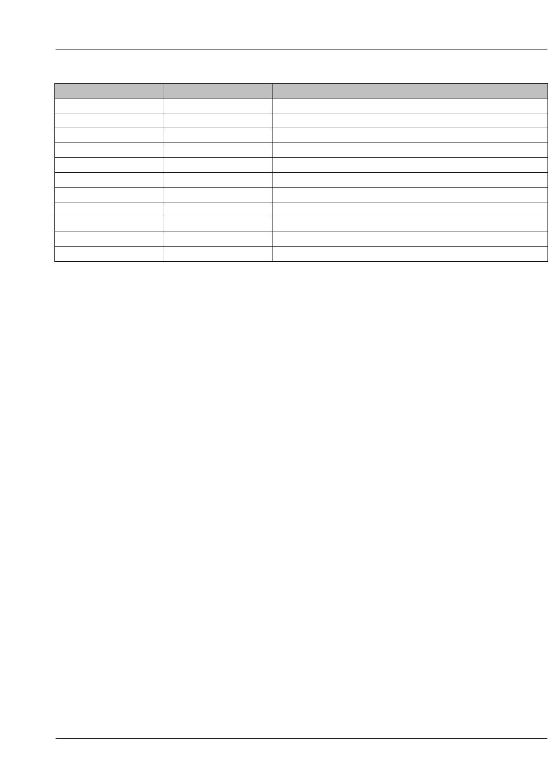
SAMSUNG Proprietary-Contents may change without notice
Main Electrical Parts List
6-17
This Document can not be used without Samsung’s authorization
SEC CODE Design LOC Discription
GH70-03349A SC109 IPR SHIELD-CAN CLIP
GH70-03349A SC110 IPR SHIELD-CAN CLIP
GH70-03349A SC113 IPR SHIELD-CAN CLIP
GH70-03349A SC114 IPR SHIELD-CAN CLIP
GH70-03349A SC116 IPR SHIELD-CAN CLIP
GH70-03349A SC117 IPR SHIELD-CAN CLIP
GH70-03349A SC118 IPR SHIELD-CAN CLIP
GH71-06721A ANT100 NPR-ANT CONTACT
GH71-06721A ANT101 NPR-ANT CONTACT
GH71-06721A ANT102 NPR-ANT CONTACT
GH71-06721A ANT103 NPR-ANT CONTACT
Please consult the GSPN website (Samsung Portal) for the most recent version of the product’s
part list.
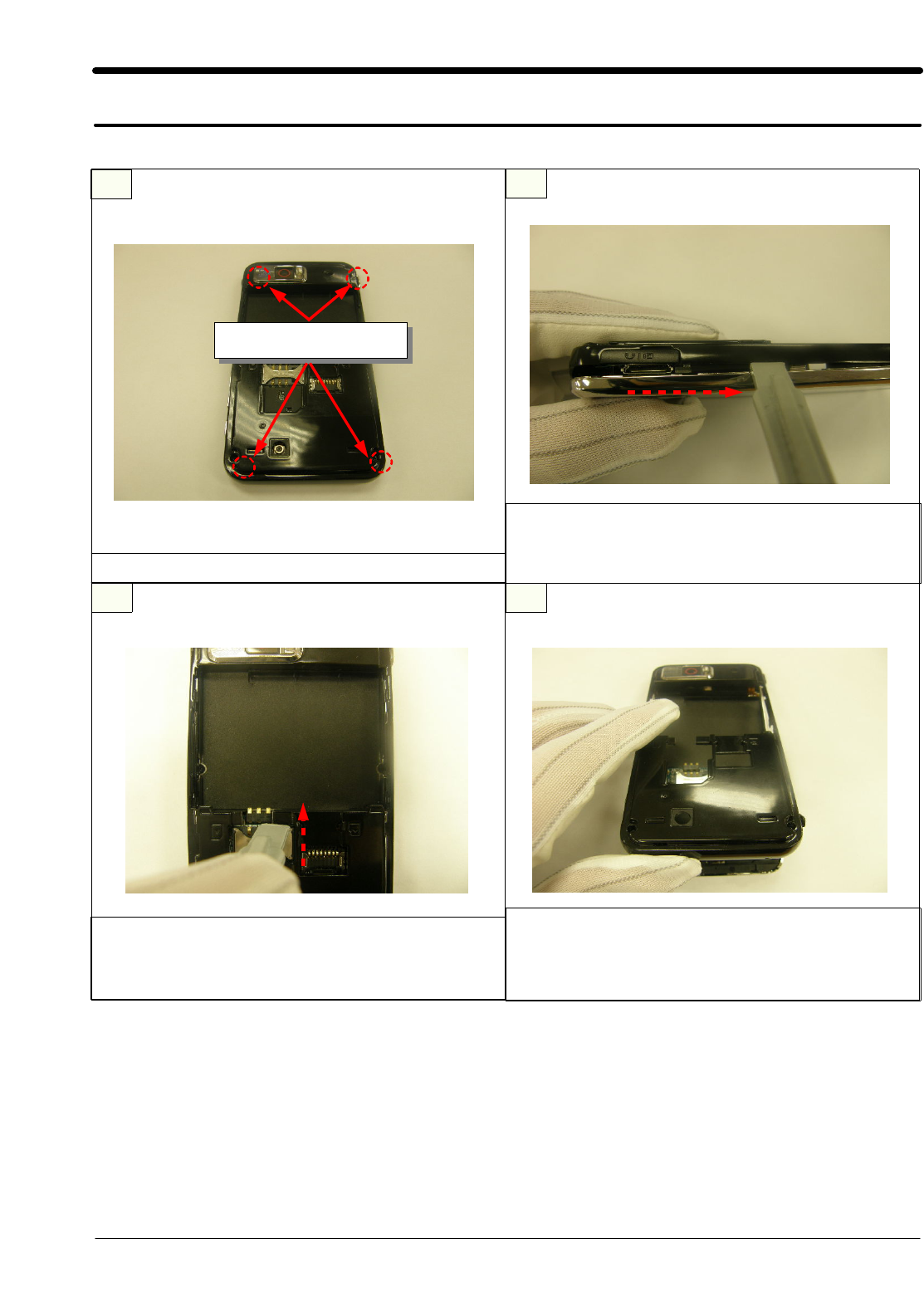
SAMSUNG Proprietary-Contents may change without notice
7. Disassembly and Assembly Instructions
7-1
This Document can not be used without Samsung’s authorization
7-1. Disassembly
1
43
2
1) UNSCREW 4REAR Points.
Separate the REAR cover -1
—Separate the rear case using adisassembly tool
following indicated direction.
Separate the REAR cover -2
—Separate the REAR using adisassembly tool
following indicated direction.
Lift the REAR from the FRONT Ass`y.
—Separate the REAR from the FRONT Ass`y with
care.
UNSCREW 4POINTS
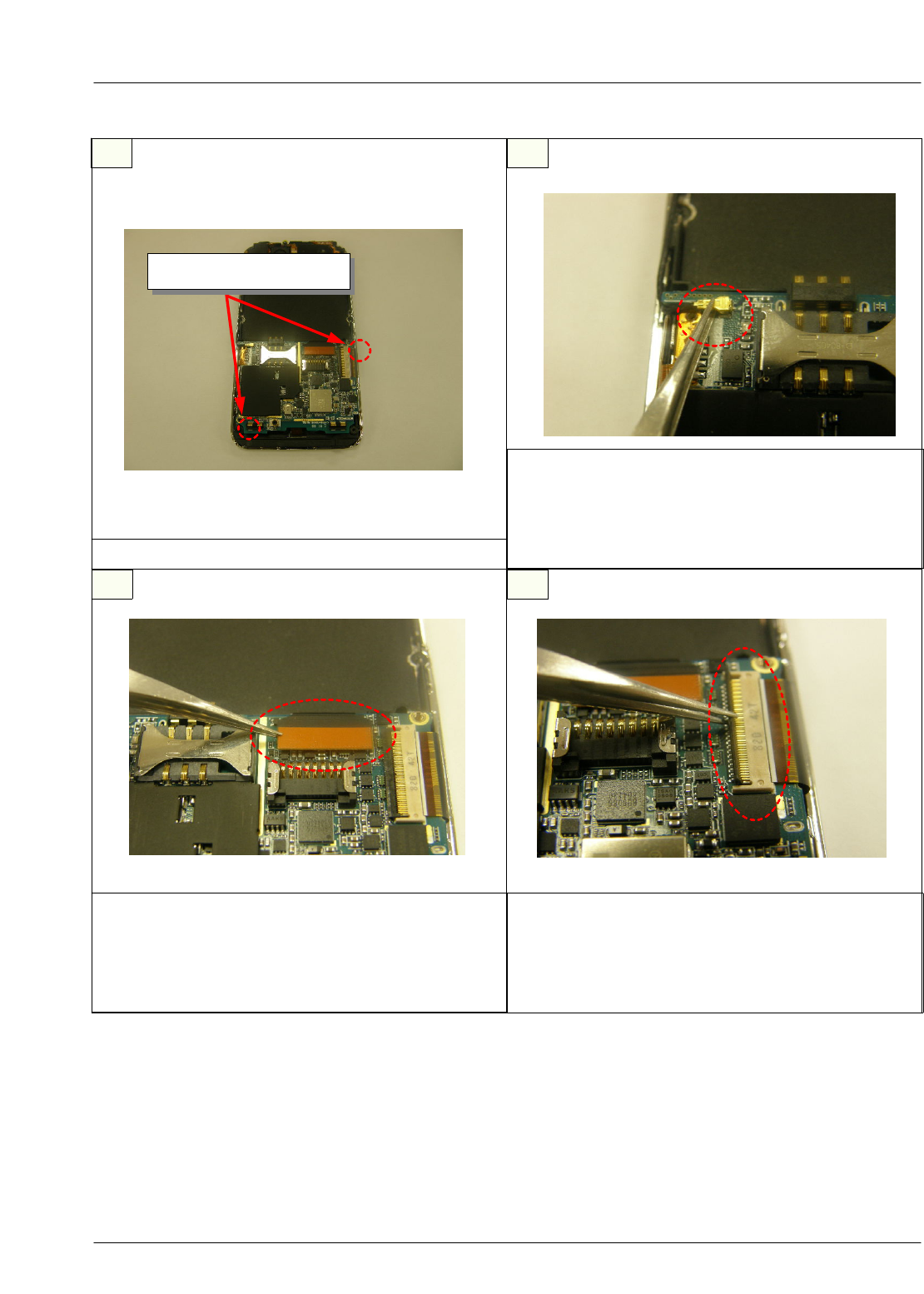
SAMSUNG Proprietary-Contents may change without notice
Exploded View and Parts List
7-2
This Document can not be used without Samsung’s authorization
5
87
6
Separate Main FPCB CONNECTOR.
—Separate Main FPCB Connector from the PBA
Connector with great care. (Be careful not to
damage FPCB &nearby chipsets.)
Separate LCD FPCB CONNECTOR.
—Separate LCD FPCB Connector from the PBA
Connector with great care. (Be careful not to
damage FPCB &nearby chipsets.)
UNSCREW PBA 2Points.
Separate GPS CONNECTOR.
—Separate GPS Connector from the PBA
Connector with great care. (Be careful not to
damage FPCB &nearby chipsets.)
UNSCREW 2POINTS
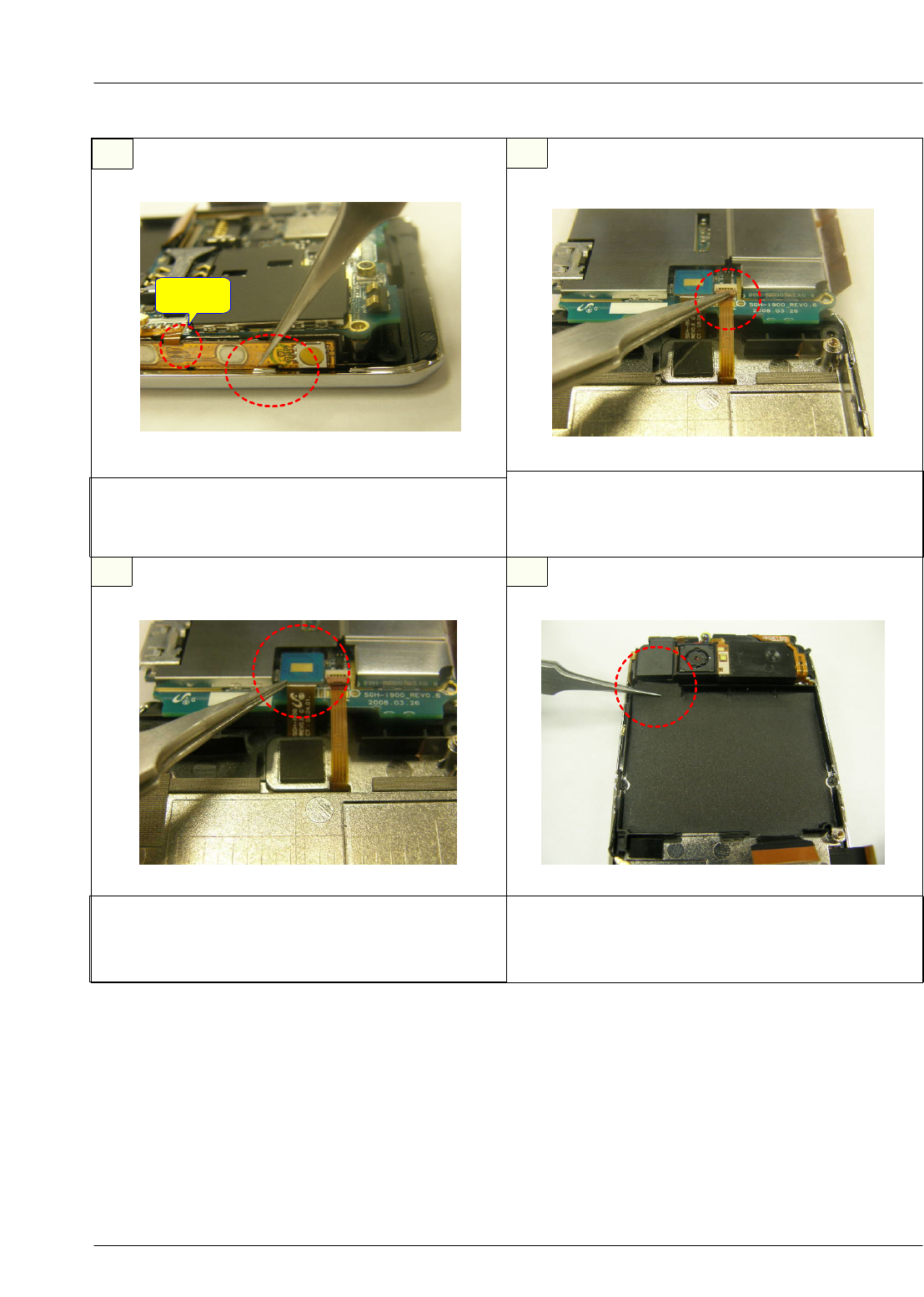
SAMSUNG Proprietary-Contents may change without notice
Exploded View and Parts List
7-3
This Document can not be used without Samsung’s authorization
9
1211
10
Separate OJ(Optical Joystic) KEY FPCB.
—Separate OJ KEY with great care not to tear OJ
KEY FPCB.
Remove Bracket Sheet.
—Remove Bracket sheet with great care not to
damage GPS wire &MAIN FPCB.
Separate VOLUME KEY FPCB.
—Separate Volume Key from PBA.
(Be careful not to damage VOLUME KEY FPCB)
Separate TSP FPCB.
—Separate TSP FPCB from PBA not to tear
FPCB with great care.
Caution!
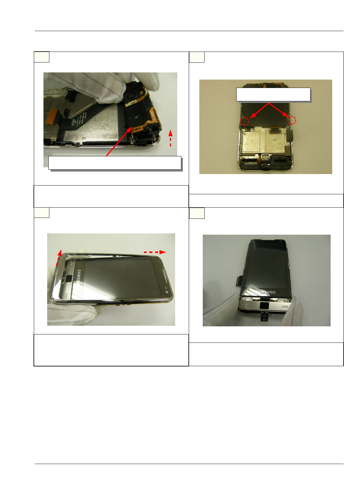
SAMSUNG Proprietary-Contents may change without notice
Exploded View and Parts List
7-4
This Document can not be used without Samsung’s authorization
13
16
15
14
Separate FRONT.
—Separate FRONT from FRONT Ass`y following
indicated direction.
Separate Key Pad.
—Separate Key Pad from FRONT Ass`y.
Separate SPK Bracket.
—Lift SPK Bracket from FRONT Ass`y. UNSCREW FRONT 2Points.
Bracket Disassembly :refer to 5/6 page
UNSCREW 2POINTS
①②
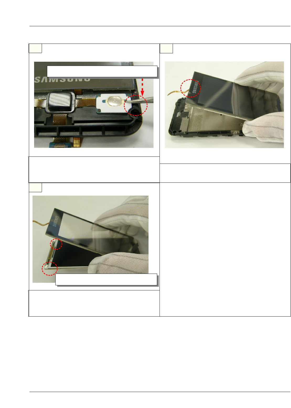
SAMSUNG Proprietary-Contents may change without notice
Exploded View and Parts List
7-5
This Document can not be used without Samsung’s authorization
17
19
18
Separate LCD from TSP.
—Separate LCD from TSP with great care not to
damage TSP.
Separate TSP Module.
—Separate TSP Module from PBA with care.
use this point to separate OJ Key easily
use this point to separate LCD easily
Separate OJ(Optical Joystic) KEY FPCB..
—Separate FPCB from FRONT Ass`y using guide
hole.
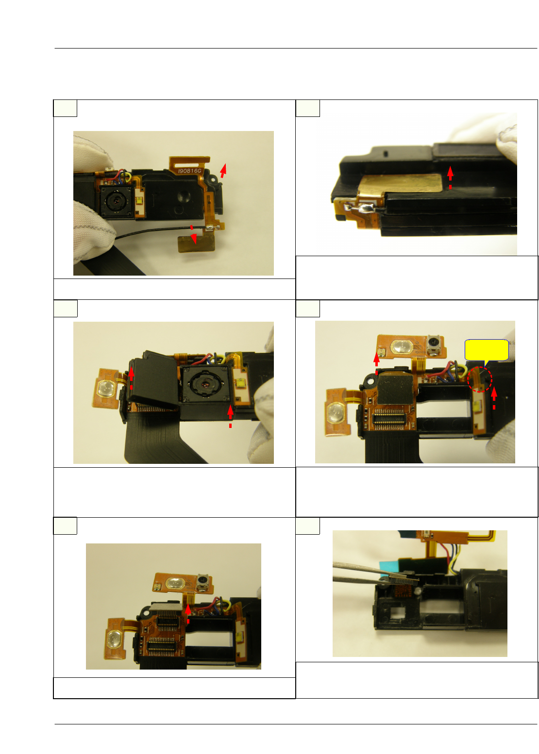
SAMSUNG Proprietary-Contents may change without notice
Exploded View and Parts List
7-6
This Document can not be used without Samsung’s authorization
7-2. SPK Disassembling
1
43
2
Disassemble 5M CAM CONNECTOR.
—Separate 5M CAM Connector First. Then Pull 5M
CAM out of Bracket.
Detach Flash FPCB &Power Key.
—Caution :Detach Flash FPCB from Bracket with
great care not to tear FPCB.
Detach GPS FPCB &GPS wire -2.
—Detach metal part of FPCB &GPS wire from
SPK Bracket.
Detach GPS FPCB -1.
①
②
Caution!
65
Disassemble CIF CAM CONNECTOR.
Separate Main FPCB from SPK Bracket &Remove
CIF CAM.
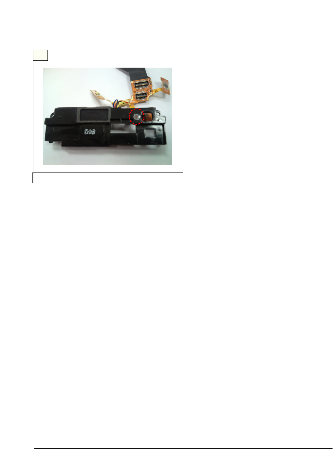
SAMSUNG Proprietary-Contents may change without notice
Exploded View and Parts List
7-7
This Document can not be used without Samsung’s authorization
7
Disassemble Window Deco.
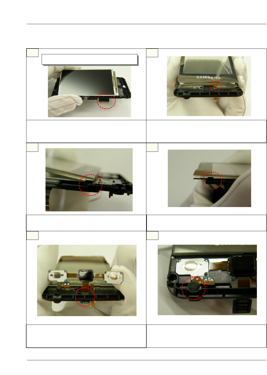
SAMSUNG Proprietary-Contents may change without notice
Exploded View and Parts List
7-8
This Document can not be used without Samsung’s authorization
7-3. Assembling
1
43
2
Attach LCD to the Main Shield Can.
—Insert LCD connector into the hole and then
attach LCD to the main shield can.
InsertTSPFPCBintothehole.
—Insert TSP FPCB into the smaller hole of the
Two.
Attach TSP on the LCP -1.
—Attach TSP referring to the Guide.
Attach TSP on the LCP -2.
—Attach TSP referring to the Guide.
Attach the left side of LCD first.
65
Insert OJ Key FPCB into the hole.
—Insert OJ(Optical Joystic) Key FPCB into the
larger hole of the Two.
Attach OJ Key on the Main Shield Can.
—Attach OJ Key referring to the Guide.
—MIC should fit in the hole.
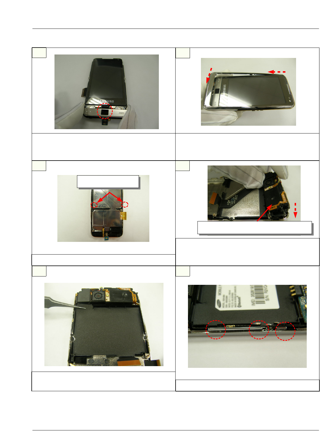
SAMSUNG Proprietary-Contents may change without notice
Exploded View and Parts List
7-9
This Document can not be used without Samsung’s authorization
7
109
8
Assemble Key Pad with OJ Key.
—Optical Joystic should fit in the hole of
Key Pad.
Assemble FRONT with FRONT Ass`y.
—Assemble FRONT with FRONT Ass`y following
indicated direction.
Screw 2FRONT Points.
Attach SPK Bracket.
—Attach SPK Bracket on the FRONT Ass`y referring
to the Guide.
1211
Attach Bracket Sheet.
—Attach Bracket sheet considering guide line. Put the GPS wire into FRONT Ass`y Guide.
①
②
SCREW 2POINTS
Bracket Assembly :refer to 5/6 page
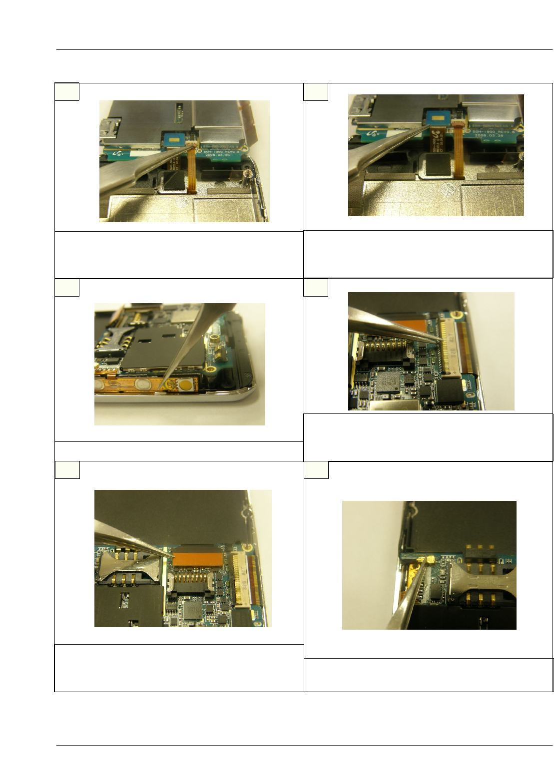
SAMSUNG Proprietary-Contents may change without notice
Exploded View and Parts List
7-10
This Document can not be used without Samsung’s authorization
13
1615
14
Assemble TSP FPCB CONNECTOR.
—Assemble TSP FPCB Connector with PBA
Connector.
Assemble OJ Key FPCB CONNECTOR.
—Assemble OJ Key FPCB Connector with PBA
Connector.
Attach Volume Key FPCB to FRONT Ass`y.
Assemble LCD FPCB CONNECTOR.
—Assemble LCD FPCB Connector with PBA
Connector.
1817
Assemble Main FPCB CONNECTOR.
—Assemble Main FPCB Connector with PBA
Connector.
Assemble GPS CONNECTOR.
—Assemble GPS Connector with PBA Connector.
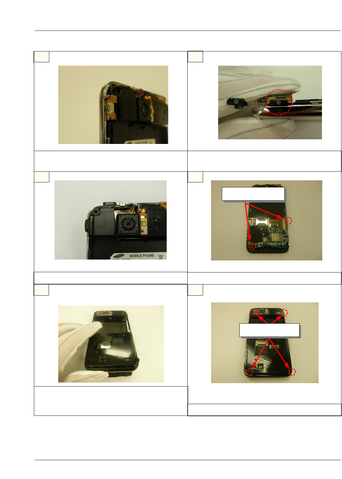
SAMSUNG Proprietary-Contents may change without notice
Exploded View and Parts List
7-11
This Document can not be used without Samsung’s authorization
19
2221
20
Put the Fuction Key FPCB into FRONT Ass`y
Guide.
Assemble Window Function key -1.
—The Rounded part is headed to the TOP.
Assemble Window Function key -2. Screw 2PBA Points.
2423
Assemble the REAR with FRONT Ass`y.
—Assemble REAR with FRONT Ass`y considering
GPS wire, Window Fuction key and IF cover. Screw 4REAR Points.
SCREW 2POINTS
SCREW 4POINTS
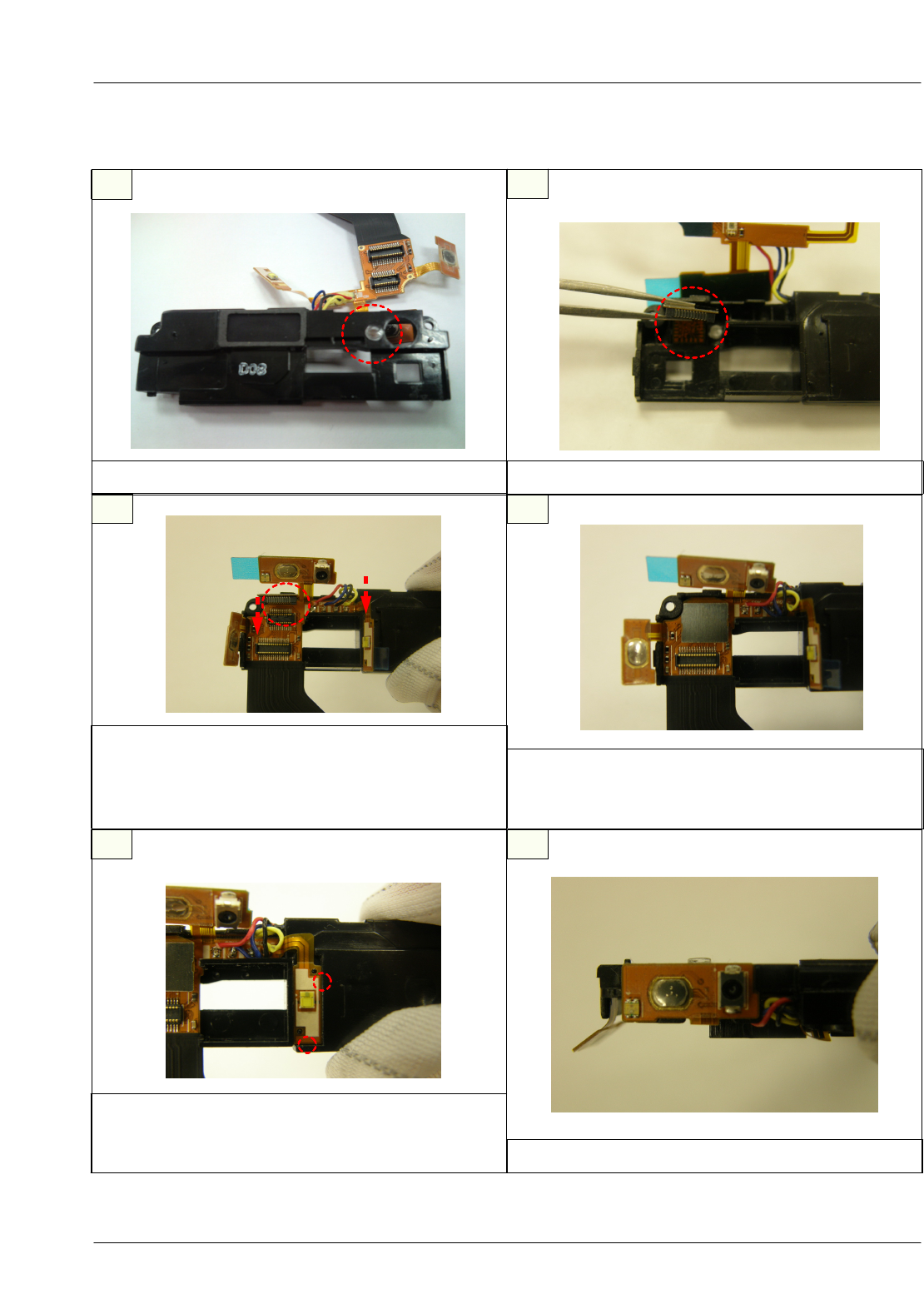
SAMSUNG Proprietary-Contents may change without notice
Exploded View and Parts List
7-12
This Document can not be used without Samsung’s authorization
7-4. SPK Assembling
1
43
2
Assemble Window Deco. Assemble CIF CAM.
Make Main FPCB fit in SPK Bracket.
—Attach Main FPCB between CIF CAM and its
Connector. Main FPCB should be stuck on SPK
Bracaket inside.
Assemble CIF CAM CONNECTOR.
—Assemble CIF CAM Connector with PBA
Connector.
65
Attach Flash FPCB.
—Attach Flash FPCB to SPK Bracket referring to
the Guide. Attach Power Key.
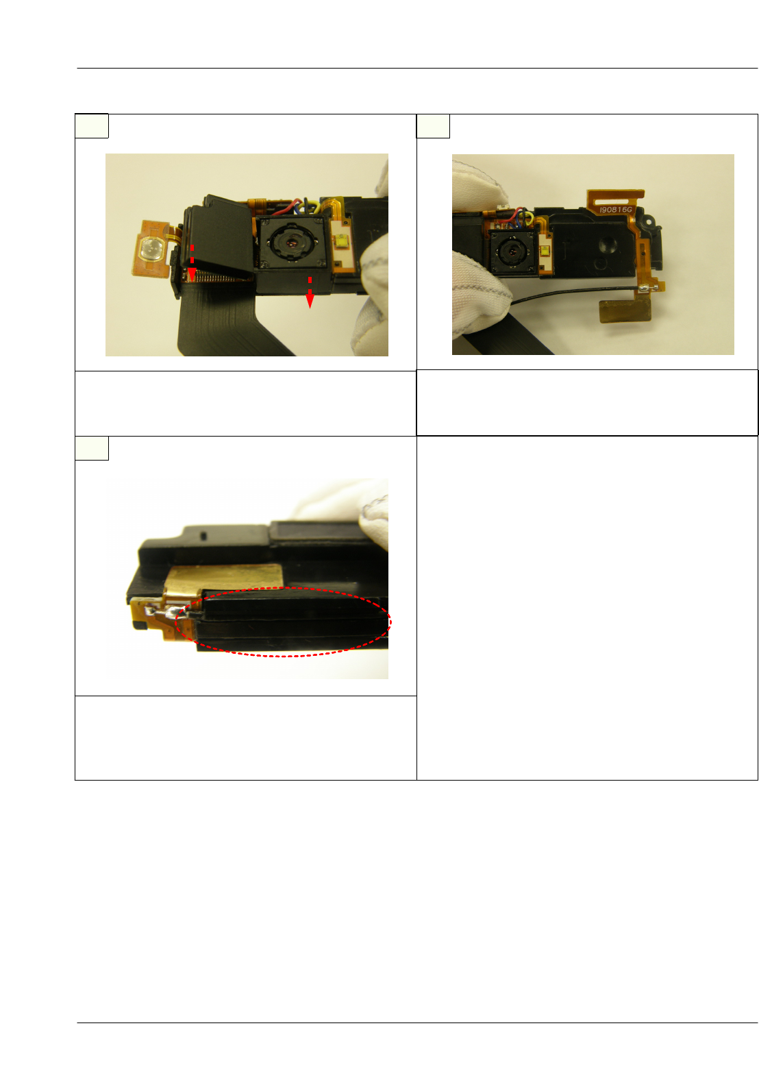
SAMSUNG Proprietary-Contents may change without notice
Exploded View and Parts List
7-13
This Document can not be used without Samsung’s authorization
7
9
8
Assemble 5M CAM CONNECTOR.
—Assemble 5M CAM Connector with FPCB
Connector following indicated direction.
Attach GPS FPCB -1.
—Attach GPS FPCB to SPK Bracket referring to
the Guide.
Attach GPS FPCB &wire -2.
—Attach metal part of FPCB to SPK Bracket
behind. Then Put GPS Wire into SPK Bracket
Guide.
①
②
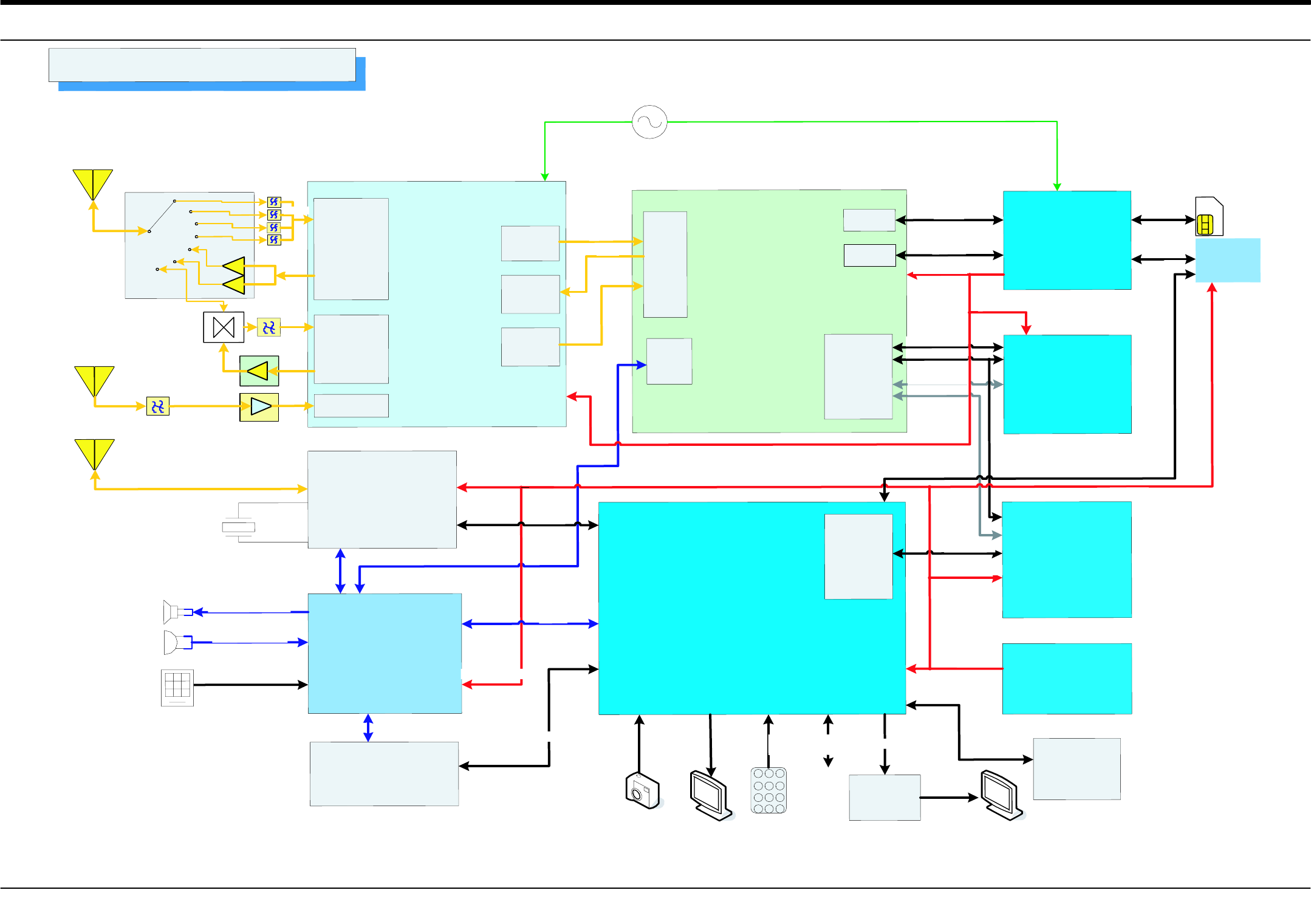
SAMSUNG Proprietary-Contents may change without notice
This Document can not be used without Samsung’s authorization
8. Block Diagrams
8-1
9
1
5
7
7
Y
K
S
R
T
R
5
8
2
6
G
5
.
2
k
c
o
l
B
F
R
S
T
M
U
k
c
o
l
B
F
R
S
P
G
A
S
P
G
Q
I
Q
I
x
T
Q
I
x
R
8
5
6
6
M
P
2
0
N
T
—
4
2
6
C
1
W
G
B
—
2
A
—
2
1
3
P
A
8
8
m
a
r
g
a
i
D
k
c
o
l
B
0
0
9
i
—
H
G
S
3
1
7
9
M
W
y
r
o
m
e
M
n
i
a
M
A
C
D
8
5
2
1
D
5
K
0
9
0
A
—
M
A
R
P
D
1
—
6
1
A
8
2
1
X
M
D
Y
D
C
M
A
P
G
5
.
2
h
c
t
i
w
S
/
.
t
n
A
n
i
a
M
N
A
L
w
/
T
B
C
Y
J
S
U
1
E
E
B
L
1
8
2
6
M
S
M
y
r
o
m
e
M
F
/
I
k
c
o
l
B
o
i
d
u
A
F
/
I
F
/
I
M
I
S
F
R
F
/
I
k
c
o
l
B
9
1
3
3
B
S
U
.
t
n
A
S
P
G
x
T
G
5
.
2
x
R
G
3
x
T
G
3
x
R
S
P
G
C
I
M
P
_
P
A
L
T
E
0
6
6
8
X
A
M
.
t
n
A
N
A
L
w
/
T
B
o
i
d
u
A
M
C
P
F
/
I
h
c
u
o
T
Q
I
x
R
Q
I
S
P
G
Q
I
x
T
F
/
I
o
i
d
u
A
F
/
I
M
I
S
F
/
I
B
S
U
O
/
I
M
I
S
F
/
I
B
S
U
O
/
I
B
S
U
)
1
3
—
0
(
1
D
_
M
S
M
)
5
1
—
0
(
2
D
_
M
S
M
)
2
1
—
0
(
1
A
_
M
S
M
)
3
1
—
1
(
2
A
_
M
S
M
y
r
o
m
e
M
F
/
I
k
c
o
l
B
)
5
1
—
0
(
O
I
_
F
D
M
S
M
_
r
e
w
o
P
r
e
w
o
P
F
R
_
h
s
a
l
F
_
r
e
w
o
P
P
A
_
r
e
w
o
P
M
A
R
P
D
_
r
e
w
o
P
N
A
L
w
/
T
B
_
r
e
w
o
P
C
E
D
O
C
_
r
e
w
o
P
B
S
U
_
r
e
w
o
P
a
t
a
D
B
S
U
N
A
L
w
/
T
B
a
t
a
D
d
n
u
o
S
a
t
a
D
t
u
p
t
u
O
P
E
/
r
e
k
a
e
p
S
t
u
p
n
I
C
I
M
r
a
E
/
C
I
M
D
C
L
a
t
a
d
M
A
C
a
t
a
d
C
789
456
123
*0#
y
e
K
t
u
p
n
i
.
m
e
M
.
t
x
E
F
/
I
x
R
G
5
.
2
O
I
D
A
R
M
F
M
G
—
6
1
B
—
3
0
7
4
I
S
L
/
R
O
I
D
A
R
C
2
I
V
T
0
0
2
2
E
S
I
T
U
O
V
T
T
U
O
V
T
l
a
n
r
e
t
n
I
y
r
o
m
e
M
)
B
G
6
1
/
B
G
8
(
z
H
M
2
.
9
1
O
X
C
T
z
H
M
6
2
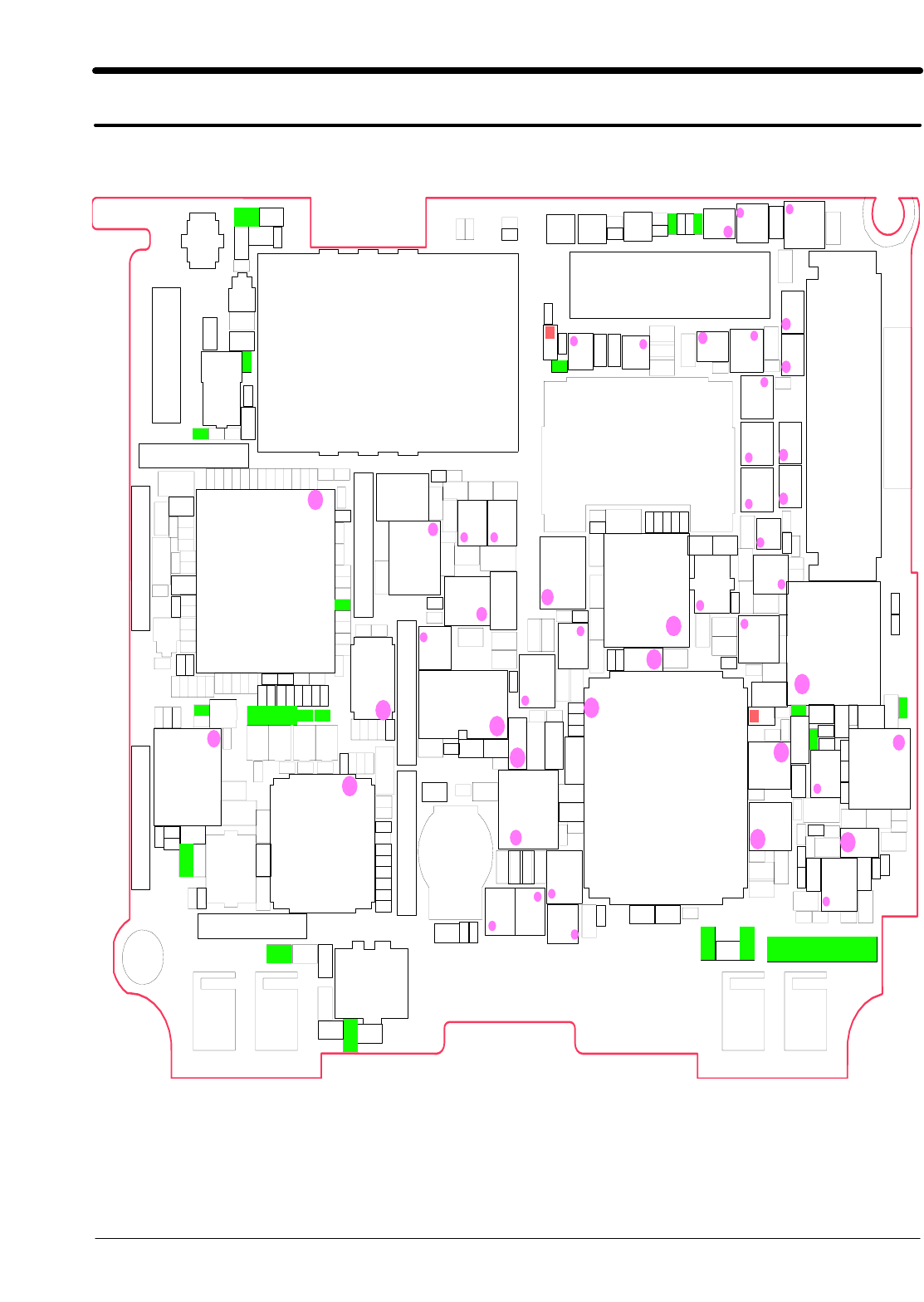
SAMSUNG Proprietary-Contents may change without notice
9. PCB Diagrams
9-1
This Document can not be used without Samsung’s authorization
0
0
1
T
N
A
1
0
1
T
N
A
2
0
1
T
N
A
3
0
1
T
N
A
0
0
3
T
A
B
1
P
T
—
6
3
T
T
—
2
U
R
4
1
4
L
M
O0
0
6
E
L
O
H
H
T
1
0
6
E
L
O
H
H
T
O
B
0
0
1
C
1
0
1
C
2
0
1
C
C103
C105
6
0
1
C
C107
C108
9
0
1
C
0
1
1
C
1
0
1
1
C
2
0
1
1
C
C1104 C1105
6
0
1
1
C
7
0
1
1
C
8
0
1
1
C
9
0
1
1
C
1
1
1
C
0
1
1
1
C
1
1
1
1
C
C1112
3
1
1
1
C
4
1
1
1
C
C112
C113
C114
C115
C116
7
1
1
C
C118
C119
C120
C121
C122
3
2
1
C
4
2
1
C
C125
6
2
1
C
7
2
1
C
8
2
1
C
9
2
1
C
C130
1
3
1
C
C132
C133
4
3
1
C
C135
C136
7
3
1
C
8
3
1
C
9
3
1
C
0
4
1
C
1
4
1
C
2
4
1
C
3
4
1
C
4
4
1
C
C145
6
4
1
C
7
4
1
C
8
4
1
C
9
4
1
C
C150
C151
C152
3
5
1
C
4
5
1
C
C155
6
5
1
C
C157
C159
C160
C161
C162
3
6
1
C
4
6
1
C5
6
1
C
C166
C167
C168
9
6
1
C
C170
C171
C172
C173
4
7
1
C
C175
6
7
1
C
C177
8
7
1
C
9
7
1
C
0
8
1
C
C181
2
8
1
C
3
8
1
C
4
8
1
C
C185
6
8
1
C
C187
C188
C189
C190
C191
C192
C193
C194
C195
C196
C197
8
9
1
C
9
9
1
C
C323
C328
9
2
3
C
0
3
3
C
C404
0
1
4
C
C411
C412
2
3
4
C
3
3
4
C
C434
C435
C438
9
3
4
C
C440
C442
C443
4
4
4
C
C445C446
7
4
4
C
8
4
4
C
C449
C450
C451
C452 C454
5
5
4
C
6
5
4
C
C457
C458
C459
C469
0
7
4
C
C500
3
0
5
C
4
0
5
C
5
0
5
C
6
0
5
C
7
0
5
C
8
0
5
C
9
0
5
C
C510
C511
C512
3
1
5
C
C517
C518
C519
C520
C521
3
2
5
C
C524
5
2
5
C
C526
C527
0
3
5
C
C531
C532
3
3
5
C4
3
5
C
C535
C537 C538
C540
1
4
5
C
2
4
5
C3
4
5
C
4
4
5
C
C546
7
4
5
C
C548
C549
C634
C635
C636
C637
C644
5
4
6
C
7
4
6
C
C649
0
5
6
C
8
5
6
C9
5
6
C
C660
1
6
6
C
C662
C680
1
8
6
C
CN301
7004—08—800
CN601
0
0
1
P
U
D
0
0
1
F
1
0
1
F
2
0
1
F
3
0
1
F
4
0
1
F
F105
7
0
1
F
8
0
1
F
0
0
5
F1
0
5
F
2
0
5
F3
0
5
F
F504
F505
2
0
5
C
P
F
HDC500
1
0
5
C
D
H
3
D
—
N
B
2
1
R
—
A
5
4
—
2
1
F
F
0
0
1
L
L101
2
0
1
L
3
0
1
L
4
0
1
L
5
0
1
L
6
0
1
L
7
0
1
L
L108
9
0
1
L
0
1
1
L
1
1
1
L
L112
4
1
1
L
5
1
1
L
L116
7
1
1
L
8
1
1
L
L119
L121
L122
3
2
1
L
4
2
1
L
L125
6
2
1
L
L402
4
0
4
L
5
0
4
L
6
0
4
L
7
0
4
L
9
0
4
L
0
1
4
L
0
0
5
L
L501
L502 L503
4
0
5
L
0
0
6
L
L601
0
0
1
D
O
M
C
Y
J
S
U
1
E
E
B
L
OSC100
’FA—128[38.4MHZ,10PPM]’
OSC101
’FCX-06[26MHZ,10PPM]’
2
0
1
C
S
O
A
1
3
—
H
L
0
1
0
5
—
G
T
0
0
1
M
A
P
1
1
—
9
1
5
7
7
Y
K
S
1
0
1
M
A
P
0
7
1
7
7
Y
K
S
R100
R101
R102
R103
R104
5
0
1
R
R106
R107
R108
R109
0
1
1
R
R111
R112
6
1
1
R
R117
R118
9
1
1
R
0
2
1
R
1
2
1
R
2
2
1
R
R123
R124
7
2
1
R
R129
5
3
1
R
R137
8
3
1
R
R139
1
4
1
R
R306
R317
9
1
3
R
0
2
3
R
1
2
3
R
2
2
3
R
3
2
3
R
R400
8
1
4
R
7
1
4
R
9
1
4
R
1
2
4
R
0
2
4
R
R423
4
2
4
R
R430
1
3
4
R
2
3
4
R
R433
4
3
4
R
5
3
4
R
R436
0
0
5
R
1
0
5
R
2
0
5
R
6
0
5
R
R507
R508
R509
R510
1
1
5
R
R512
R513
R514
R515
7
1
5
R
8
1
5
R
9
1
5
R
0
2
5
R
R604
6
0
6
R
8
0
6
R
7
0
6
R
R631
RFS100
1
0
1
S
F
R
2
0
1
C
S
SC103
4
0
1
C
S
7
0
1
C
S
9
0
1
C
S
0
1
1
C
S
SC111
SC116
SIM300
PC-D6-A3-H2.7-S-M
TA100
TA406
7
0
4
A
T
0
0
5
R
T
1
0
5
R
T
2
0
5
R
T
U100
RTR6285
U101
MIC5335—SGYMT
U306
U308
ESDALC6V1—5M6
9
0
3
U
2
1
3
U
6
M
5
—
1
V
6
C
L
A
D
S
E
U400
DG2011
U401
RP150K010A-TR
U402
S1M0080X01-P070
U405
SI4703—B16—GM
U407
MAX4744ELBT
U408
MAX4744ELBT
U500
BD6086GU
2
0
5
U
E
S
5
0
—
8
1
2
1
M
C
U503
NC7SV74L8X
U504
NC7SV74L8X
U505
MAX3373EEKA-T
U506
AAT1270IFO
7
0
5
U
4
0
1
G
T
—
A
U
E
7
3
2
1
X
A
M
8
0
5
U
R
T
—
A
2
0
0
K
0
5
1
P
R
U509
MIC5335-MMYMT
U510
ISA1000
1
1
5
U
2
1
T
X
E
Y
0
4
6
8
X
A
M
U512
MIC5335-MGYMT
4
1
5
U
T
M
Y
P
S
—
0
2
3
5
C
I
M
U515
NC7SV74L8X
U516
NC7SV08L6X
U601
MIC5330-PGYML
8
0
6
U
X
8
L
8
0
P
W
7
C
N
U609
NC7WP08L8X
4
0
6
D
C
U
0
0
2
2
E
S
I
VR300
VR500
ZD403
ZD404
ZD405
0
0
5
D
Z
ZD501
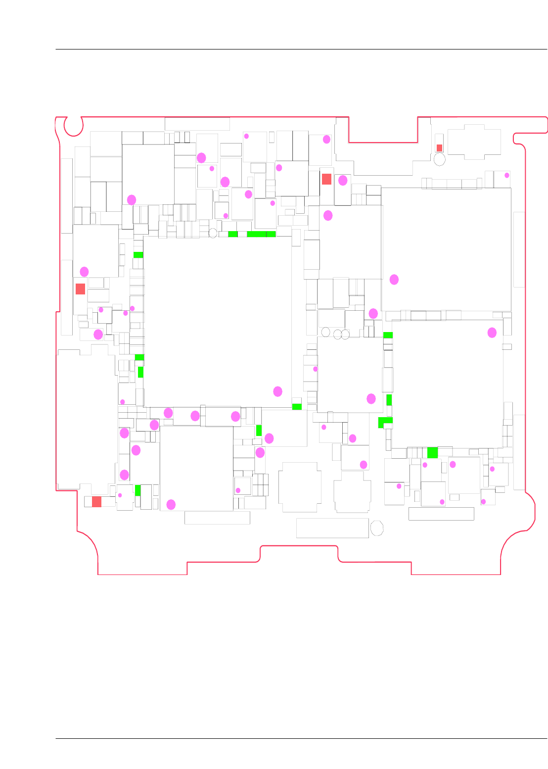
SAMSUNG Proprietary-Contents may change without notice
PCB Diagrams
9-2
This Document can not be used without Samsung’s authorization
BTC300
C200
1
0
2
C
C202
3
0
2
C
4
0
2
C
5
0
2
C
C206
C207
C208
9
0
2
C
C210
C211 C212
C213
C214
5
1
2
C
6
1
2
C
7
1
2
C
C218
9
1
2
C
0
2
2
C
1
2
2
C
2
2
2
C
3
2
2
C
4
2
2
C
C225C226
7
2
2
C
8
2
2
C
9
2
2
C
1
3
2
C
C232
3
3
2
C
4
3
2
C
5
3
2
C
C236
7
3
2
C
8
3
2
C
C239
C240
1
4
2
C
2
4
2
C
3
4
2
C
C244
5
4
2
C
6
4
2
C
0
0
3
C
1
0
3
C
2
0
3
C
C303C304
C305
6
0
3
C
C307
8
0
3
C
C309
C310
C311
2
1
3
C
C313
C314
C315
C316
C317
8
1
3
C
C319
0
2
3
C
1
2
3
C
C322
4
2
3
C
5
2
3
C
6
2
3
C
C327
1
3
3
C
0
0
4
C
C401
2
0
4
C
3
0
4
C
C405 C406 C407
C408
C409
C413C414
C415
C416
C417
8
1
4
C
9
1
4
C
0
2
4
C
1
2
4
C
C422
C423
4
2
4
C
5
2
4
C
C426
7
2
4
C
8
2
4
C
9
2
4
C
C453
C461
C462
5
6
4
C
6
6
4
C
7
6
4
C
C468
C600
C601
2
0
6
C
3
0
6
C
C604
C605
C606
C607
8
0
6
C
9
0
6
C
C610
C611
2
1
6
C
3
1
6
C
C614
C615
C616
7
1
6
C
C618
C619
C620
C621
C622
C623
C624
5
2
6
C
6
2
6
C
7
2
6
C
8
2
6
C
C629
C630
1
3
6
C
C632
C633
8
3
6
C
C639
0
4
6
C
C641
2
4
6
C
C643
6
4
6
C
C648
C651
2
5
6
C
3
5
6
C
C654
C655
6
5
6
C
7
5
6
C
3
6
6
C
4
6
6
C
5
6
6
C
C666
7
6
6
C
8
6
6
C
C669
0
7
6
C
C671
2
7
6
C
C673
4
7
6
C
5
7
6
C
C676
7
7
6
C
C678
C679
2
8
6
C
1
0
2
N
C
D300
1
0
3
D
D302
0
0
6
D
E
L
A
_
F
D
DF_CLE
E
_
K
L
C
S
_
F
D
HDC201
HDC400
AXK816145SJ
0
0
4
C
F
I
5
0
—
0
2
0
0
—
0
0
2
1
0
0
3
L
1
0
3
L
2
0
3
L
2
0
6
L
3
0
6
L
L604
L605
MGND
0
0
3
C
S
O
5
1
3
M
C
0
0
4
C
S
O
Z
H
M
6
9
0
.
4
—
F
C
S
0
1
3
—
G
S
OSC600
CX-4025S
OSC601
CM315
R200
2
0
2
R
6
0
2
R
R207
8
0
2
R
9
0
2
R
R210
R211
R212
R213
4
1
2
R
5
1
2
R
6
1
2
R
7
1
2
R
R218
9
1
2
R
R220
1
2
2
R
2
2
2
R
0
0
3
R
R302
3
0
3
R
R304
R307
R309
R310
R311
2
1
3
R
R313
4
1
3
R
R315
6
1
3
R
R318
1
0
4
R
R402
3
0
4
R
4
0
4
R
R405
6
0
4
R
7
0
4
R
8
0
4
R
R409
0
1
4
R
1
1
4
R
2
1
4
R
4
1
4
R
5
1
4
R
R425
R426
7
2
4
R
8
2
4
R
R600
R601
R602
3
0
6
R
5
0
6
R
R610
1
1
6
R
2
1
6
R
3
1
6
R
R614
5
1
6
R
R616
R617
R618
9
1
6
R
0
2
6
R
R621
R622
3
2
6
R
4
2
6
R
R625
6
2
6
R
R627
R628
0
3
6
R
0
0
1
C
S1
0
1
C
S
SC106
SC113
4
1
1
C
S
SC117
8
1
1
C
S
SLC501
0
0
3
A
T
TA400
TA401 TA402
3
0
4
A
T
4
0
4
A
T5
0
4
A
T
TA600
TP_CBL_PWR_N
TP_PSHOLD
0
0
6
R
T
U200
U201
NC7SV08L6X
2
0
2
U
R
T
—
A
6
0
0
K
0
5
1
P
R
3
0
2
U
X
8
L
8
0
P
W
7
C
N
U204
FXLP34L6X
5
0
2
U
L
5
8
E
T
—
U
F
4
0
H
S
7
C
T
U206
’TC7SH32FU[TE85L]’
7
0
2
U
X
8
L
4
7
V
S
7
C
N
U208
ESDALC6V1—5M6
U300
NLAS5223BMNR2G
1
0
3
U
8
5
6
6
M
P
U302
AAT4280IJS—3—T1
3
0
3
U
X
8
7
0
4
C
T
L
U304
MIC94062BC6
U305
R3111Q301C-TR
U307
NC7WP08L8X
U310
R3111Q311C-TR
1
1
3
U
X
6
L
9
1
Z
S
7
C
N
9
0
4
U
G
B
T
T
M
E
A
8
4
3
P
C
N
U600
FXLP34L6X
2
0
6
U
X
6
L
8
0
V
S
7
C
N
U603
USB3319-CP-TR
U605
MAX8660ETL-T
7
0
6
U
0
2
0
A
M
B
U610
NC7WP08L8X
UCD402
WM9713LGEFL/RV
UCP200
MSM6281_NSP
0
0
6
P
C
U
2
0
N
T
—
4
2
6
C
1
W
G
B
—
2
A
—
2
1
3
P
A
8
8
UME200
K5D1258DCA-A090
UME201
CYDMX128A16—65BVXI
1
0
2
D
Z
ZD300
ZD400
ZD401
2
0
4
D
Z
ZD406
SAMSUNG Proprietary-Contents may change without notice
10. Flow Chart of TroubleShooting
10-1
This Document can not be used without Samsung’s authorization
10-1. Power On
zPDA Part
No
‘Power On’
Voltage in U605
V1=3.0
V2=1.8
V3=1.4
V4=1.4
V5=1.8
V5=1.8
Battery Change
Check U605 &Neighboring Circuit
No
Yes
No
At TA300
V>3.32
Yes
1,4 Pins in U304
V1 =V4
Yes
Check U304 &Neighboring Circuit
No
Check other Power Devices
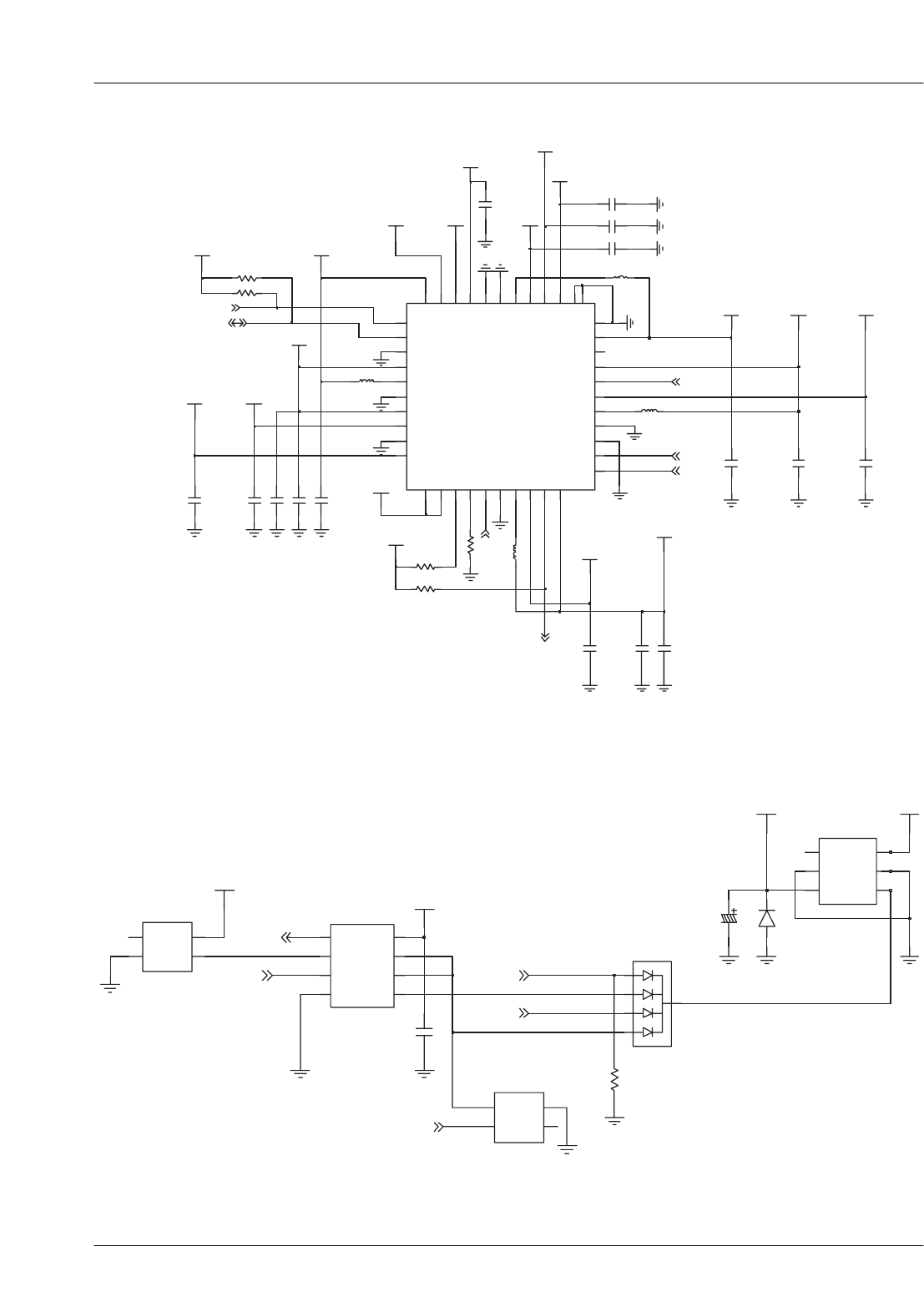
SAMSUNG Proprietary-Contents may change without notice
Flow Chart of Troubleshooting
10-2
This Document can not be used without Samsung’s authorization
VCODEC_2.0V
0
7
6
C
4
7
6
C
3
7
6
C
2
7
6
C
VCC_1.4V_APPS
VBATT
VCC_1.4V_SRAM
5
7
6
C
VCC_3.0V
VCC_1.8V
8
6
6
C
VCC_3.0V
VBATT
VBATT
3
2
6
R
VCC_TV_3.0V
6
7
6
C
7
7
6
C
C665
VBATT
L603
R624
R626
VBATT
VBATT
L602R619
3
2
9
2O
S
R
_
0
1
0
33
V
0
4
V4
2
5
V
7
6
V
9
7
V
0
2
V8
3
1
_LBO
R
M
_
4
X
L
P
M
A
R
4
2
SCL
1
1
SDA
2
1
9
3
SET1
6
2
T
E
S
3
3
SRAD
8
3
V1
2
V
4
3
PG1
PG2
6
1
3
G
P
6
24
G
P5
PV1
6
3
PV2
4
1
8
23
V
P3
4
V
P
4
IN8
1
2F
B
L
R
B
L
2
2
5
3
LX1
LX2
5
1
3
X
L
7
2
C
N2
4
3
4
C
N
2
3
EN34
1
3
5
N
E
5
2
9
1
GND
GND
1
4
IN
8
1
1
5
N
I
7
6
N
I8
7
1
U605
7
3
EN1
EN2
1
7
6
C
VCC_1.8V_SYS
R620
VBATT
C663
VBATT
VCC_3.3V_BATT
C666
7
6
6
C
VCC_3.3V_BATT
C664
L604
9
6
6
C
N
E
_
S
Y
S
SYS_EN
SYS_EN
PWR_EN
N
I
_
T
S
R
n
PWR_SDA
PWR_SCL
R316
TA300
GND 4
3
NC
OUT
1
VDD
2
U310
U305
4GND
NC
3
1
OUT
2
VDD
VBATT
D301
B1 6
2B2
GND
4
VCC 8
Y1
1
5
Y2
U307
A1 7
A2
3
VIN
1
VOUT
U304
EN 3
GND 2
GND
5
6NC
4
VCC_3.3V_BATT
VBATT
V_DC
C327
1
2
3
4
5
D302
ON_SW
nPOWER
VEXT_5VPS_HOLD
IF_CON_SENSE
SAMSUNG Proprietary-Contents may change without notice
Flow Chart of Troubleshooting
10-3
This Document can not be used without Samsung’s authorization
0
0
3
C
1
0
3
C2
0
3
C
C303C304
C305
C311
4
2
3
C
5
2
3
C
6
2
3
C
C327
1
3
3
C
C453
2
0
6
C
3
0
6
C
8
C615
7
C618 C619C622
5
2
6
C
6
2
6
C
8
1
3
6
6
C
4
6
6
C
5
6
6
C
C666
C669
0
7
6
C
C671
2
7
6
C
C673
4
7
6
C
5
7
6
C
C676
1
0
3
D
D302
2
0
6
L
3
0
6
L
L604
L605
R309
R310
R311
R313
4
1
3
R
R315
6
1
3
R
R318
8
2
4
R
9
1
6
R
0
2
6
R3
2
6
R
4
2
6
R
6
2
6
R
0
3
0
0
3
A
T
U302
3
0
3
U
U304
U305
U307 U310
1
1
3
U
9
0
4
U
U605
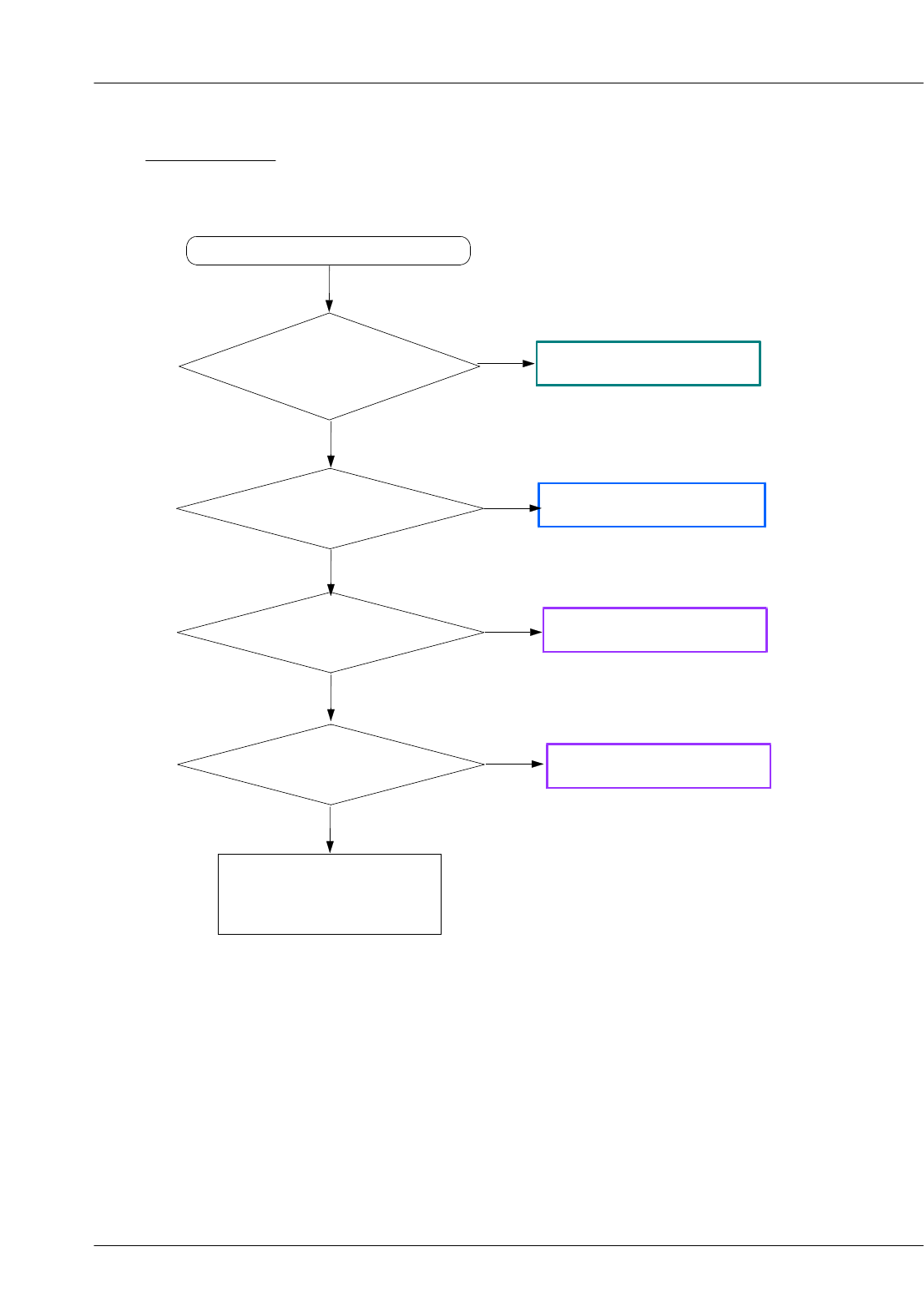
SAMSUNG Proprietary-Contents may change without notice
Flow Chart of Troubleshooting
10-4
This Document can not be used without Samsung’s authorization
zPHONE Part
`
2PininD300
Low
Phone on
4Pin in U201
Low
Check UME201& Neighboring circuit
Check U201 &Neighboring Circuit
Yes
No
No
No
Yes
Yes
3PininD300
Low Check D300
Check U301& Neighboring Circuit
Output PWR
U301
O.K?
No
No
Yes
Check OSC102 &UCP 600
Neighboring Circuit
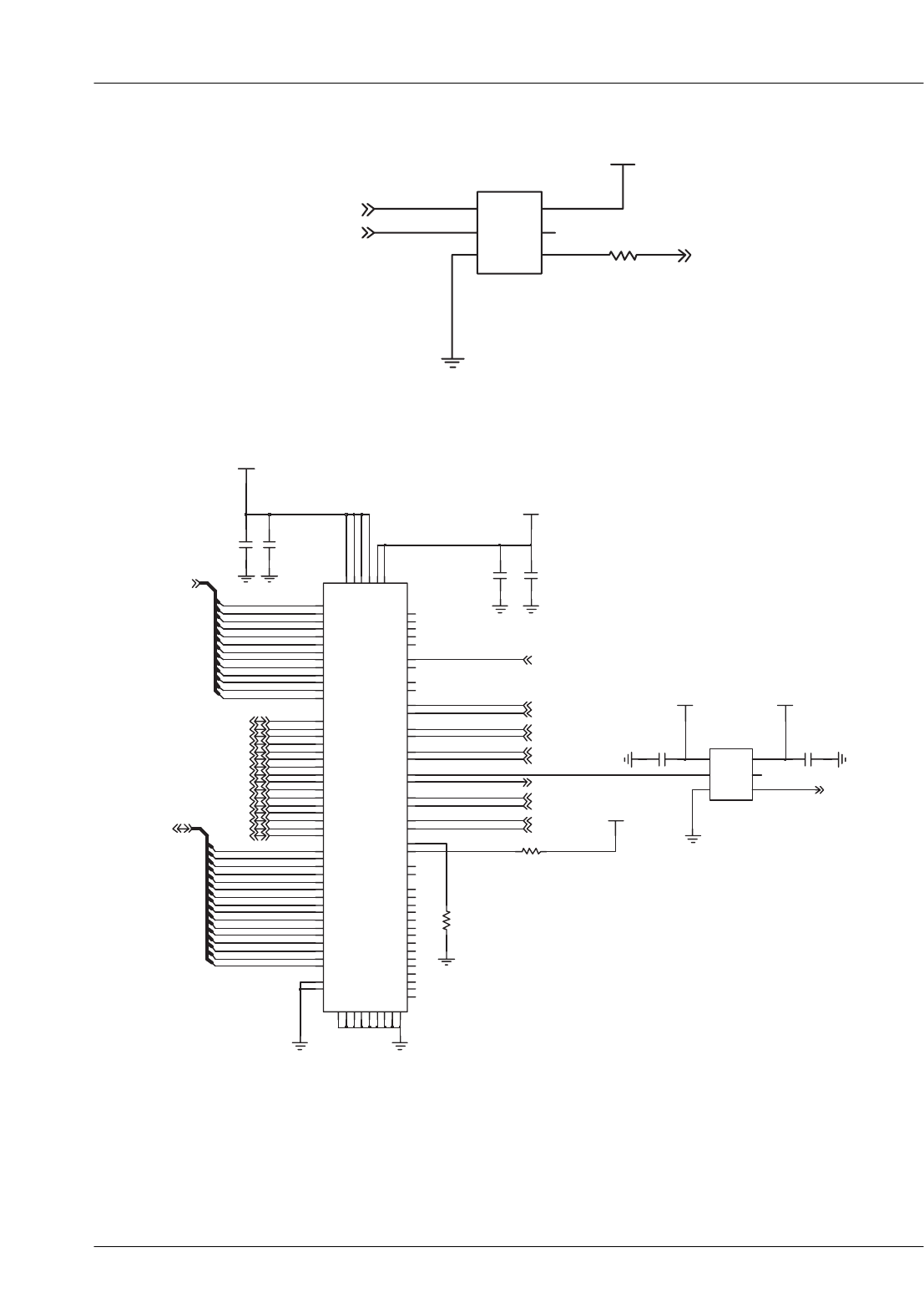
SAMSUNG Proprietary-Contents may change without notice
Flow Chart of Troubleshooting
10-5
This Document can not be used without Samsung’s authorization
R200
U201
1A
B
2
3GND
5
NC
6
VCC
4
Y
VCC_2.8V
PON_RST_PMIC_N
FONE_RST
PON_RST_PDA_N_O
5
3
2
C
3
3
2
C
R219
VCC_3.0V
6
3
2
C
R220
DNU K3
UB_L K4
ADV_L K5
WE_L K6
I|OL0
K7
I|OL2
K8
I|OL5
K9
C
C
V5
J
S
S
V
6
J
I|OL4
J7
I|OL6
J8
I|OL8
J9
DNU K1
I|OL7
K10
DNU K2
L
O
I
D
D
V7
H
MSEL H8
DNU H9
DNU J1
I|OL9
J10
DNU J2
DNU J3
IRR0 J4
I|OL14
G9
DNU H1
I|OL10
H10
DNU H2
DNU H3
LB_L H4
CE_L H5
I|OL1
H6
I|OL13
G10
DNU G2
DNU G3
DNU G4
OE_L G5
I|OL3
G6
I|OL11
G7
I|OL12
G8
BUSY_L F3
DNU F4
C
C
V5
F
S
S
V
6
F
I|OR3
F7
I|OR0
F8
I|OL15
F9
ODR0 G1
S
S
V
5
E
S
S
V
6
E
I|OR4
E7
R
O
I
D
D
V8
E
I|OR1
E9 SFEN F1
L
O
I
D
D
V0
1
F
ODR1 F2
I|OR13
D7
I|OR8
D8
I|OR5
D9
S
S
V
1
E
S
S
V
0
1
E
DNU E2
ODR3 E3
INT_L E4
I|OR7
C9
ODR4 D1
I|OR2
D10
ODR2 D2
BUSY_R D3
INT_R D4
A10
D5
A12
D6
S
S
V
0
1
C
A1
C2
A2
C3
A6
C4
LB_R C5
IRR1 C6
I|OR14
C7
I|OR11
C8
A7
B3
A9
B4
CE_R B5
WE_R B6
OE_R B7
R
O
I
D
D
V8
B
I|OR9
B9
A0
C1
S
S
V
5
A
ADV_R A6
I|OR15
A7
I|OR12
A8
I|OR10
A9
A3
B1
I|OR6
B10
A4
B2
NC
1
NC
2
A5
A1
S
S
V
0
1
A
A8
A2
A11
A3
UB_R A4
UME201
4
3
2
C
VCC_2.8V
C240
VCC_1.8V
VCC_1.8V
VCC_1.8V
C239
A
3GND
NC 5
6
VCC
VCC1
1
Y4
U204
2
DPRAM_nINT_PDA
DPRAM_nINT_MSM
DPRAM_MSM_nCS
DPRAM_PDA_nCS
DF_CLE
NAND_RE
NAND_WE
DF_ALE
NAND_CLE
NAND_ALE
MSM_A2(1:13)
MSM_A2(1)
MSM_A2(3)
MSM_A2(2)
MSM_A2(4)
MSM_A2(5)
MSM_A2(6)
MSM_A2(7)
MSM_A2(8)
MSM_A2(9)
MSM_A2(10)
MSM_A2(11)
MSM_A2(12)
MSM_A2(13)
MSM_D2(11)
DF_IO1
DF_IO2
DF_IO3
DF_IO4
DF_IO5
DF_IO6
DF_IO7
DF_IO8
DF_IO9
DF_IO10
DF_IO11
DF_IO12
DF_IO13
DF_IO14
DF_IO15
MSM_D2(0:15)
MSM_D2(0)
MSM_D2(1)
MSM_D2(2)
MSM_D2(3)
MSM_D2(4)
MSM_D2(5)
MSM_D2(6)
MSM_D2(7)
MSM_D2(8)
MSM_D2(9)
MSM_D2(10)
MSM_D2(12)
MSM_D2(13)
MSM_D2(14)
MSM_D2(15)
nBE0
nBE1
nLLA
DF_IO0
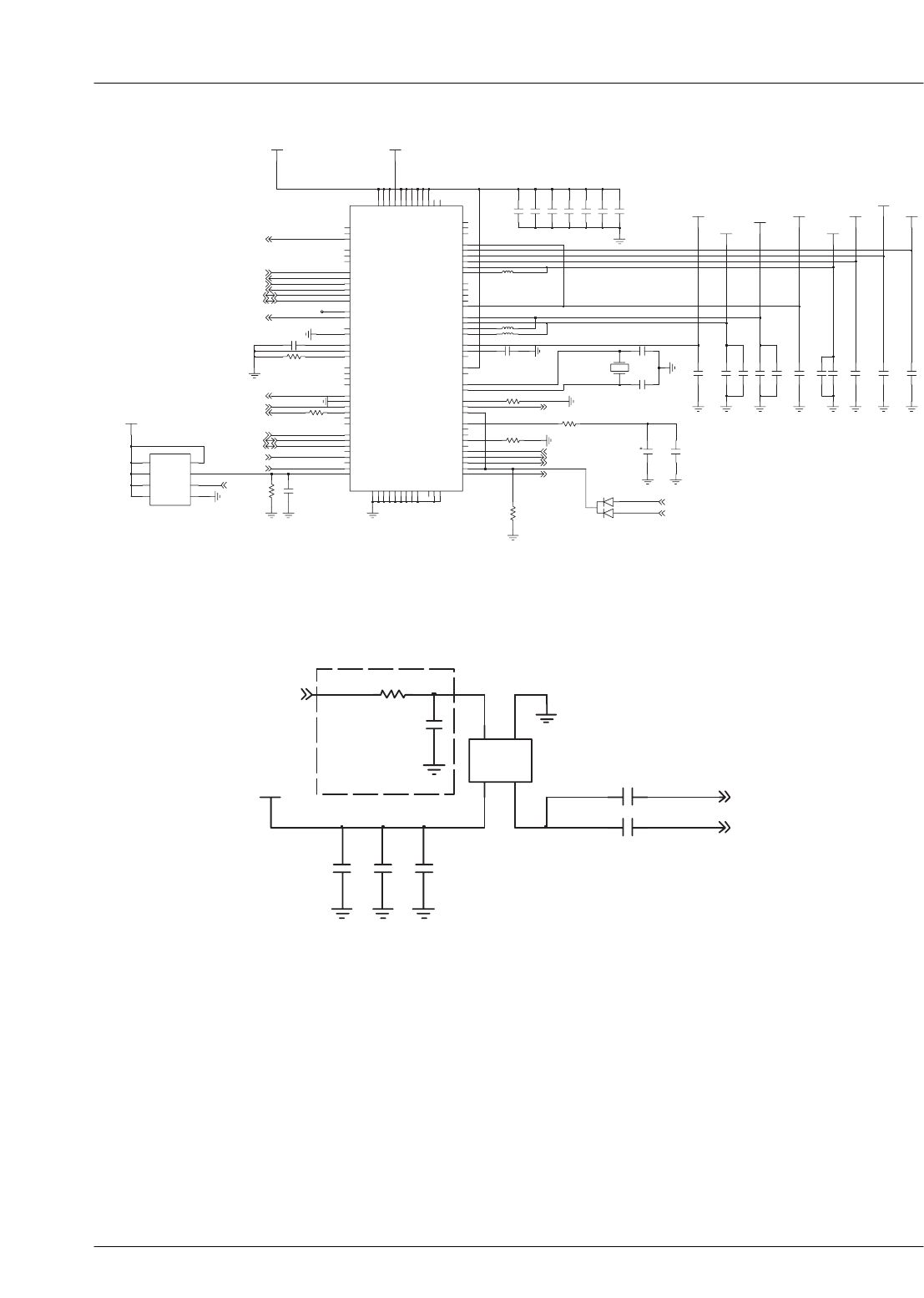
SAMSUNG Proprietary-Contents may change without notice
Flow Chart of Troubleshooting
10-6
This Document can not be used without Samsung’s authorization
L300
R306
5
1
3
C
VMSME_1.8V
VRFRX2_2.7V
R303
9
1
3
C
C308
V6.2_PMSMVV58.2_OXCTV
3
1
2
3
0
3
C
D300
TP_CBL_PWR_N
C309
4
1
3
C
5
0
3
C
C317
C
2
1
3
C
3
1
3
C
R307
V
3
.
6
VUSB_5V
8
1
3
C
1
0
3
C
0
2
3
C
1
2
3
C
VMSMC_1.2V
OSC300
R304
L3 MPP3|VIB_DRV_N
L4
KPD_PWR_N
5
L
C
M
S
M
_
D
D
V
L6
VREG_S3
7
L
3
2
S
_
D
D
V
L8
VREG_S2
L9
VREG_MMC
K6
VSW_S3
K7
VSW_S2
K8
VREG_MSME
K9
SLEEP_CLK
L1 MPP4|LCD_DRV_N
L10
VREG_RUIM
L11
XTAL_IN
L2 KPD_DRV_N
J2 USB_D_P K1
HSET_BIAS
0
1
K
M
I
U
R
_
D
D
V
K11
XTAL_OUT
K2 MPP7|CBLPWR_N
K3 AMUX_OUT
K4
VREG_MSMC K5
VSW_MSMC
H4 USB_SE0
H5 MPP12|RUIM_IO
H6 MPP10|RUIM_CLK
H7 MPP6|RUIM_RST
H8 OPT_2
J1 USB_D_M
J10
VCOIN
J11
VREG_MSMP
5
GD
N
G
6
GD
N
G
7
GD
N
G
G8
SBDT|SSBI
H1 USB_VBUS
H10 TCXO_OUT_1
1
1
H
M
S
M
_
D
D
V
H2 USB_ID
7
FD
N
G
F8
SBCK
1
G
V
5
_
G
E
R
V
G10
PON_RESET_N
G11
VREG_MSMA
G2
VREG_USB
G4 USB_DAT
7
ED
N
G
E8
SBST
1
F
V
5
_
W
S
V
F10
PS_HOLD
F11 TCXO_OUT_RF
F2 USB_OVP_G
F4 USB_OE_N
5
FD
N
G
6
FD
N
G
D8 TCXO_EN_1
1
E
T
A
B
V
E10 REF_GND
E11 TCXO_IN
E2
BAT_FET_N
E4 TCXO_EN_2
5
ED
N
G
6
ED
N
G
D1
ISNS_M
D10 REF_ISET
1
1
DC
N
D
D2
ISNS_P
D4 OPT_1
D5 MPP11|RUIM_M_IO
D6 MPP9|RUIM_M_CLK
D7 MPP5|RUIM_M_RST
B6 SPKR_IN_P
B7 MPP2|AMUX_IN2
B8
VREG_RFUBM
9
B
F
R
_
D
D
V
C1
VCHG
C10
MSM_INT_N
C11 REF_BYP
C2
CHG_CTL_N
B1
VREG_GP3
B10 TCXO_OUT_2
B11
VREG_WLAN
2
B
N
I
A
M
_
D
D
V
3
B
P
G
_
D
D
V
B4 MPP8|REF_OUT
B5 SPKR_IN_M
1
1
A
N
A
L
W
_
D
D
V
A2
VREG_GP2
A3
VREG_GP1
4
A
R
K
P
S
_
D
D
V
A5 SPKR_OUT_M
A6 SPKR_OUT_P
A7 MPP1|AMUX_IN1
A8
VREG_RFTX
A9
VREG_RFRX1
U301
1C
N
2C
N
A1
VREG_TCXO
A10
VREG_RFRX2
VMSMA_2.6V
ON/_OFF 3
OUT 2
4
GND
IN 1
5IN
IN
6
7IN
IN
8
U302
C324
VRFRX1_2.1V
1
1
3
C
L302
6
0
3
C
6
1
3
C
VRFRX2_2.7V
V_DC
0
0
3
C
R302
4
0
3
C
2
2
3
C
3
2
3
C
2
0
3
C
1
2
0
0
3
T
A
B
R312
VUSIM_3.0V
L301
R309
TCXO_EN
TCXO_OUT
REF_OUT
PS_HOLD_F
PON_RST_PMIC_N
PM_INT_N
AMUX_OUT
TCXO
PM_SIM_RST
PM_SIM_CLK
PM_SIM_IO
USB_OE_MSM
USB_DAT_MSM
USB_SEO_MSM
PHONE_D+
PHONE_D-
PHONE_DEBUG_ON
PS_HOLD_F
nPHONE_ON
SIM_CLK
SIM_IO
SIM_RST
SBDT
SLEEP_CLK
Place near the TCXO
C1109
2
GND
3
OUT
1
VC
VCC
4
OSC102
6
0
1
1
C
R135
C1104
C1105
7
0
1
1
C
8
0
1
1
C
VTCXO_2.85V
TRK_LO_ADJ
RTR6285_TCXO
TCXO
SAMSUNG Proprietary-Contents may change without notice
Flow Chart of Troubleshooting
10-7
This Document can not be used without Samsung’s authorization
BTC300
C200
1
0
2
C
C202
3
0
2
C
4
0
2
C
5
0
2
C
C206C207
C208
9
0
2
C
C210
C211 C21 2
C213
C214
5
1
2
C
6
1
2
C
7
1
2
C
C218
9
1
2
C
0
2
2
C
1
2
2
C
2
2
2
C
3
2
2
C
4
2
2
C
C225C226
7
2
2
C
8
2
2
C
9
2
2
C
1
3
2
C
C232
3
3
2
C
4
3
2
C
5
3
2
C
C236
7
3
2
C
8
3
2
C
C239
C240
1
4
2
C
2
4
2
C
3
4
2
C
C244
5
4
2
C
6
4
2
C
0
0
3
C
1
0
3
C2
0
3
C
C303C30 4
C305
6
0
3
C
8
0
3
C
C309
C310
C311
2
1
3
C
C313
C314
C315
C316
C317
8
1
3
C
C319
0
2
3
C
1
2
3
C
C322
5
2
3
C
6
2
3
C
C632
C633
C641
C643
C678
C679
2
8
6
C
D300
1
0
3
D
DF_ALEDF_CLE
1
0
2
C
D
H
0
0
4
C
D
H
0
0
3
L
1
0
3
L
2
0
3
L
0
0
3
C
S
O
OSC600
R200
2
0
2
R
6
0
2
R
R207
8
0
2
R
9
0
2
R
R210
R212
R213
4
1
2
R
5
1
2
R
6
1
2
R
7
1
2
R
R218
9
1
2
R
R220
1
2
2
R
2
2
2
R
R302
3
0
3
R
R304
R307
2
1
3
R
R315
R600
R601
R602
5
1
6
R
0
0
1
C
S
1
0
1
C
S
SC113
SLC50 1
0
0
3
A
T
TP_CBL_PWR_ N
TP_PSHOLD
0
0
6
R
T
U200
U201
2
0
2
U
3
0
2
U
U204
5
0
2
U
U206
7
0
2
U
U208
U301
U304
7
0
6
U
U610
0
0
2
P
C
U0
0
2
E
M
U
UME201
1
0
2
D
Z
2
0
4
D
Z
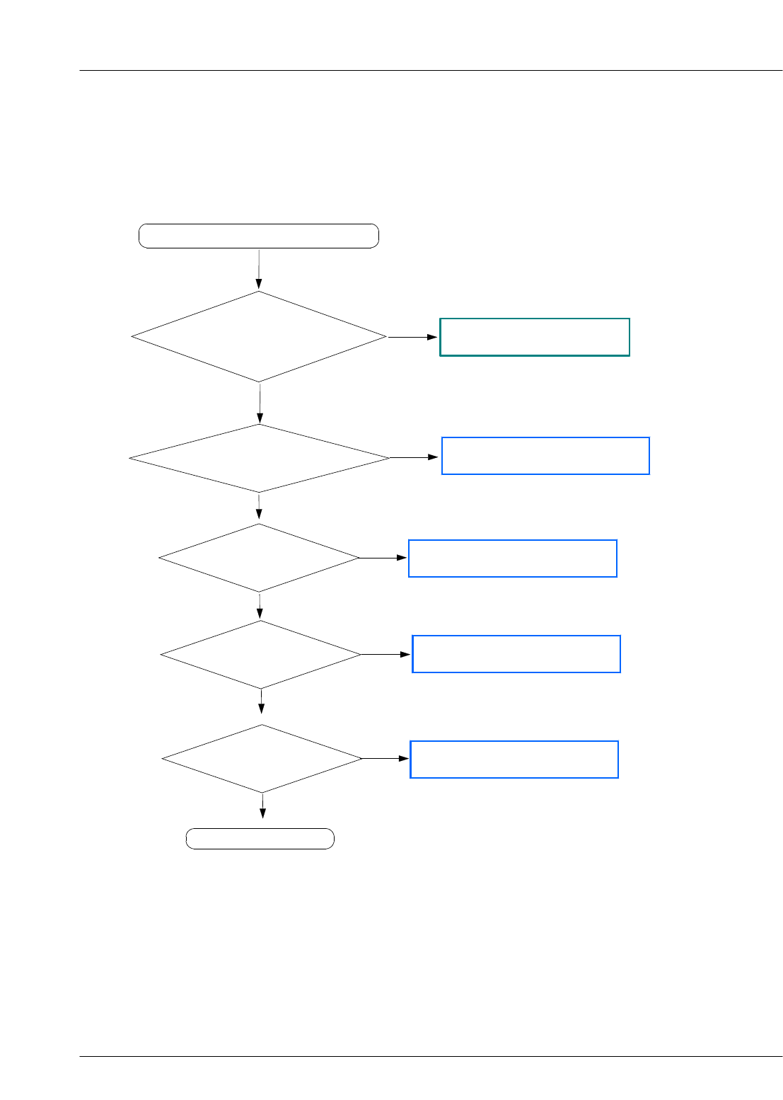
SAMSUNG Proprietary-Contents may change without notice
Flow Chart of Troubleshooting
10-8
This Document can not be used without Samsung’s authorization
10-2. RECEIVER Working
2, 4 PininU407
Signal ON ?
AE15, AE16 Pin in
UCP200
Signal ON?
Operator receive
SPK-Assy’s Breakdown?
Check UDC402, C416, C417
Change SPK-Assy’s
Yes
No
No
No
Yes
No Check PIN 6, 10 in U407
Yes
12, 14 PininU402
Signal ON ?
10, 18 PininU402
Signal ON ?
No
Check R430, R433
Yes
Check L404, L405
No
Yes
END
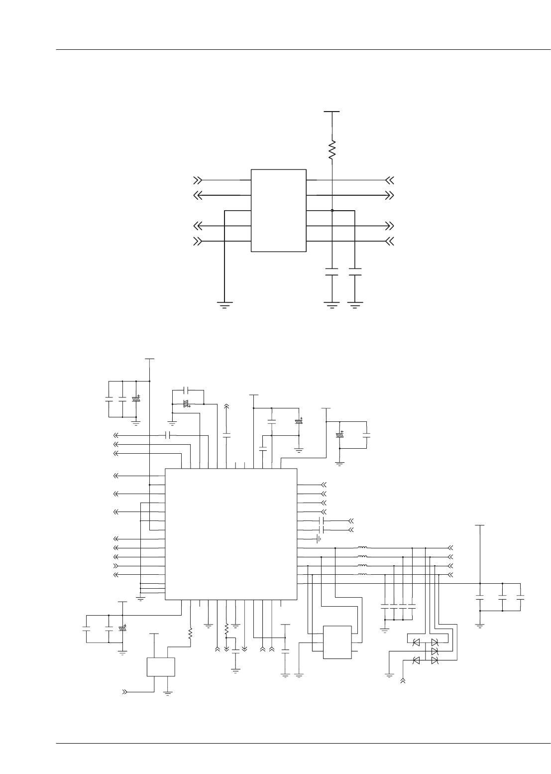
SAMSUNG Proprietary-Contents may change without notice
Flow Chart of Troubleshooting
10-9
This Document can not be used without Samsung’s authorization
C456
C455
8
5
10
COM1
COM2 6
GND
3
NC 9
7
NC
2NO1
4NO2
VCC
U407
CB1
1
CB2
VAUDIO_3.3V_A
R435
SPKL
SPK_SW
RCV_P
SPKR
CODEC_OUT_R
SPK_SW
RCV_N CODEC_OUT_L
9
2
4
C
6
ZD402
1
2
34
5
VAUDIO_3.3V_A
5
6
4
C
0
0
4
A
T
C422
C402
C405
4
IO3
IO4 5
6
IO5
C424
ZD406
2GND
IO1
1
IO2
3
8
6
4
C
6
6
4
C
C403
C428
TA403
C417
TA405
C425
VMICBIAS_2.7V
7
6
4
C
C401
VCODEC_2.0V
VAUDIO_3.0V
5
1
4
R
4
1
4
R
VAUDIO_3.3V_A
R412
C407
TA401
VAUDIO_3.0V
C427
9
6
4
C
R411
0
0
4
C
OSC400
GND
2
3
OUT
4
VDD
1
_ST
C416
R410
8
0
4
C
R409
TA402
VAUDIO_3.3V_A
5
1
Y+
7
1
Y-
6
0
4
C
8
3
SPKVDD
0
1C
N
Y
S
8
1
TPGND
3
1
TPVDD
7
2
F
E
R
V
2
14
X
U
A
/
R
E
P
I
W
4
1
X+
6
1
X-
3
3
4
T
U
O
9
1
PCBEEP
1
17
O
I
P
G
/
B
T
E
S
E
R
8N
I
A
T
A
D
S
5T
U
O
A
T
A
D
S
4
3
D
N
G
K
P
S
5
3
L
K
P
S
6
3
R
K
P
S
0
3
2
X
U
A
/
2
P
M
O
C
/
B
2
C
I
M
8
2
S
A
I
B
C
I
M
2
2
MICOM
1
3
O
N
O
M
0
2
MONOIN
0
5
NC
1
5
NC
7
3
OUT3
1
4
HPR
HPVDD
3
4
3
2
LINEL
4
2
LINER
2A
K
L
C
M
3B
K
L
C
M
1
2
MIC1
9
2
1
X
U
A
/
1
P
M
O
C
/
A
2
C
I
M
GND
4
4
9
4
GPIO1/PCMCLK
5
4
GPIO2/IRQ
6
4
GPIO3/PENDOWN/PCMFS
7
4
GPIO4/ADA/MASK/PCMDAC
8
4
GPIO5/SPDIF/PCMADC
0
4
HPGND
9
3
HPL
2
4
AGND2
5
2
D
D
V
A
6K
L
C
T
I
B
2
3
2
P
A
C
1D
D
V
B
D
9D
D
V
C
D
41
D
N
G
D
72
D
N
G
D
UCD402
6
2
D
N
G
A
K
L
C
T
I
B
TSPX
TSPY
TSMX
TSMY
CODECCLK_EN
D
N
G
_
C
C
V
_
J
O
RADIO_L
RADIO_R
MSM_SPK_N
P
_
C
I
M
_
M
S
M
EARCOM
T
U
O
_
A
T
A
D
S
C
N
Y
S
SPKL
SPKR
BT_PCM_SYNC
T
S
R
_
7
9
C
A
n
BT_PCM_CLK
BT_PCM_OUT
BT_PCM_IN
EAROUT_L
EAROUT_R
SPK_SW
MSM_SPK_P
MSM_MIC_N
MIC_P
MIC_N
N
I
_
A
T
A
D
S
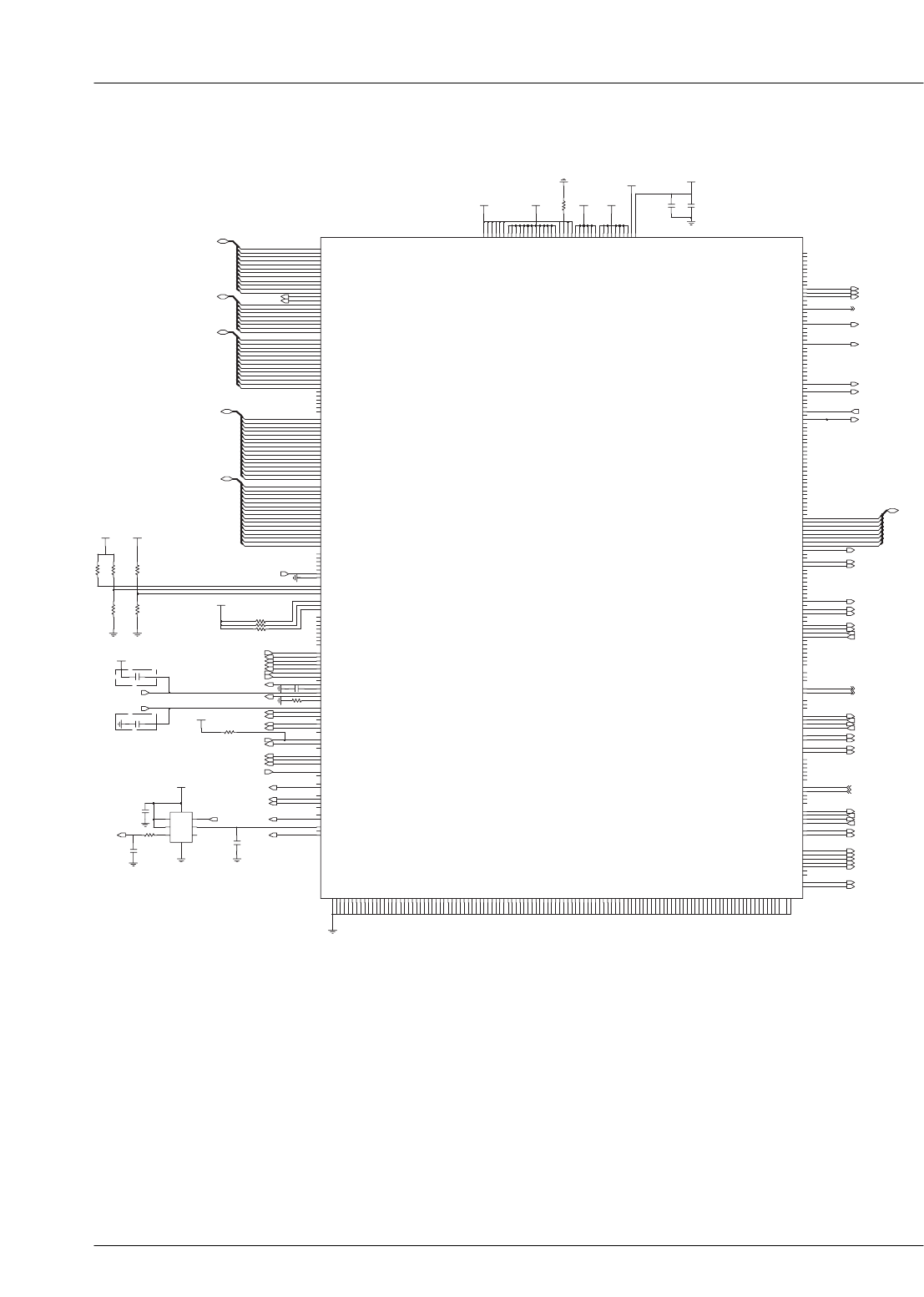
SAMSUNG Proprietary-Contents may change without notice
Flow Chart of Troubleshooting
10-10
This Document can not be used without Samsung’s authorization
Place between D12 and E12
Set Near AA22
C
N
1
1
2
R
C
N
0
1
2
R
R217
VTCXO_2.85V
VMSMA_2.6V
VMSMA_2.6V C222
C244
TP_PSHOLD
VCC
8
2
_CLR
1
_PR
_Q
5
U207
7
CK
6
D
GND
4
3
Q
NC
VMSMP_2.6V
R214
VMSME_1.8VVMSMP_2.6V
C237
C223
NCR216
9
0
2
RK
0
1
Q_IM_CH0 Y24
A
D
D
V5
2
Y
SDRAM1_D4|D1_4
Y4
SDRAM1_D2|D1_2
Y5
RESOUT_N_EBI1
W5
D
N
G
7
W
D2_2
W8
D2_8
W9
XMEM1_CS_N1|GPIO76 Y1
SDRAM1_D20|GPIO71 Y2
MODE0
Y21
HKAIN5
Y22
A
S
S
V
8
1
W
D
N
G
9
1
W
2
G
I
D
_
D
D
V2
W
HKAIN4
W21
HKAIN1
W22
Q_IP_CH0 W24
A
D
D
V5
2
W
XMEM1_CS_N3|GPIO77|SDRAM1_CS_N1 W4
D2_12
W10
D2_13
W11
A2_8
W12
A2_15
W13
XMEM2_CS_N0|NAND1_CS_N
W14
XMEM2_CS_N2|GPIO35 W15
A
S
S
V
6
1
W
HPH_L W17
I_IP_CH1 V24
A
S
S
V
5
2
V
XMEM1_CS_N0|SDRAM1_CS_N2
V4
XMEM1_HWAIT_N|SDRAM1_CLK_EN1
V5
MDP_VSYNC_PRIMA_RY|GPIO105 V7
D
N
G
8
V
D
N
G
9
V
2
G
I
D
_
S
S
V
1
W
NAND2_FLASH_READY|GPIO33|EBI2_PNAND_READY V15
MICBIAS V16
D
N
G
7
1
V
D
N
G
8
1
V
D
N
G
9
1
V
OE1_N|SDRAM_CLK_EN2
V2
HKAIN0
V21
Q_IM_CH1 V22
SDRAM1_D22|GPIO73|EBI1_HLB_N U7
D
N
G
8
U
A1_24|GPIO79SDRAM1_A0 V1
D2_5
V10
D2_9
V11
A2_3
V12
A2_7
V13
A2_18|D216ADV_N
V14
HKAIN3
U19
4
1
D
A
P
_
D
D
V2
U
KEYSENSE4_N|GPIO48|ETM_TRACE_PKT2 U21
Q_IP_CH1 U22
I_IM_CH1 U24
A
S
S
V
5
2
U
SDRAM1_D23|GPIO74|EBI1_HUB_N U4
XMEM1_CS_N2|SDRAM1_CS_N0
U5
A
D
D
V4
2
T
A
D
D
V5
2
T
SDRAM1_D17|GPIO68 T4
GPIO78|A1_23|SDRAM1_DQM2 T5
SDRAM1_D16|GPIO67 T7
A1_25|GPIO75|SDRAM1_DQM3 T8
4
1
D
A
P
_
S
S
V
1
U
D
N
G
8
1
U
A1_22|SDRAM1_D31
R7
WE1_N|SDRAM1_WE_N R8
A1_17|SDRAM1_D26
T1
E
S
U
F
Q
_
D
D
V8
1
T
A
S
S
V
9
1
T
A1_18|SDRAM1_D27
T2
GPIO9|GRFC6 T21
MODE1
T22
KEYSENSE0_N|GPIO62|KYPD_1|ETM_PIPESTAT0 R19
3
1
D
A
P
_
D
D
V2
R
GPIO20|BT_DATAETM_TRACE_PKT8 R21
MODE2
R22
6
G
I
D
_
D
D
V4
2
R
6
G
I
D
_
S
S
V
5
2
R
A1_21|SDRAM1_D30
R4 A1_20|SDRAM1_D29
R5
SDRAM1_D18|GPIO69 P8
3
1
D
A
P
_
S
S
V
1
R
D
N
G
1
1
R
D
N
G
2
1
R
D
N
G
3
1
R
D
N
G
4
1
R
D
N
G
5
1
R
UART1_CTS_N|GPIO97 R18
A1_11
P2
KEYSENSE3_N|GPIO47|KYPD_7|ETM_TRACE_PKT1 P21
GPIO10|GRFC7 P22
0
3
D
A
P
_
D
D
V4
2
P
0
3
D
A
P
_
S
S
V
5
2
P
A1_15|SDRAM1_D24
P4
A1_16|SDRAM1_D25
P5
A1_13
P7
A1_10
P1
D
N
G
1
1
P
D
N
G
2
1
P
D
N
G
3
1
P
D
N
G
4
1
P
D
N
G
5
1
P
PA_ON2|GPIO29|BM_INT|TSIF_SYNC P18
KENSENSE1_N|GPIO63|KEYSENSE1_N|KYPD_3 P19
USB_SE0_VM N21
A
D
D
V2
2
N
PA_POWER_CTL
N24
A
S
S
V
5
2
N
SDRAM1_D8|D1_8
N4
A1_12
N5
A1_7
N7
A1_19|SDRAM1_D28
N8
D
N
G
1
1
N
D
N
G
2
1
N
D
N
G
3
1
N
D
N
G
4
1
N
D
N
G
5
1
N
GPIO27|I2C_SCL N18
PA_POWER_CTL_M
N19
A1_8
N2
GPIO14|AUX_PCM_DIN|SDAC_MCLK|GRFC13|ETM_TRACE_PKT9|TSIF_NULL M22
USB_OE_TP_N M24
USB_DAT_VP M25
SDRAM1_CLK_EN0
M4
A1_5
M5
A1_6
M7
A1_14
M8
A1_9
N1
D
N
G
2
1
M
D
N
G
3
1
M
D
N
G
4
1
M
D
N
G
5
1
M
RINGER|GPIO18|CAMIF_EN M18
UART3_DP_TX_DATA|GPIO84|TSIF_ERROR|TSIF_NULL|TSIF_SYNC|PM_SBCK M19
2
1
D
A
P
_
D
D
V2
M
UART3_DP_RX_DATA|GPIO85|TSIF_DATA|PM_SBST M21
SDCC_DAT2|GPIO100 L24
SDCC_DAT3|GPIO101 L25
UB1_N|SDRAM1_DQM1 L4
A1_4
L5
A1_2
L7
A1_3
L8
2
1
D
A
P
_
S
S
V
1
M
D
N
G
1
1
MD
N
G
3
1
L
D
N
G
4
1
L
D
N
G
5
1
L
SDCC_CLK|GPIO31|MMC_CLK L18
GPIO80|AUX_PCM_CLK|ETM_TRACE_PKT10|GRFC14|TSIF_SYNC|TSIF_SYNC|TSIF_NULL L19
LB1_N|SDRAM1_DQM0 L2
SBCK|SSBI2_DATA
L21
UART1_DP_RX_DATA|GPIO96 L22
UART3_RFR_N|GPIO87|TSIF_CLK K24
UART1_DP_TX_DATA|GPIO95|NAND_BOOT_ERR K25
SDRAM1_D15|D1_15
K4
SDRAM1_D13|D1_13
K5
SDRAM1_D14|D1_14
K7
XMEM1_LWAIT_N|SDRAM1_CAS_N
K8
A1_1
L1
D
N
G
2
1
L
SDRAM1_D7|D1_7
J7
D
N
G
8
J
1
1
D
A
P
_
S
S
V
1
K
GPIO57|CAMIF_DATA5|ETM_TRACE_PKT11 K18
SDCC_DAT1|GPIO99 K19
1
1
D
A
P
_
D
D
V2
K
GPIO26|I2C_SDA K21
UART3_CTS_N|GPIO86|TSIF_ENABLE|PM_SBDT K22
GPIO21|BT_TX_RX_N|ETM_TRACE_PKT11 J19
SDRAM1_D10|D1_10
J2
GPIO13|GP_MN|GP_CLK|CAMCLK_PO J21
GPIO82|CAMIF_PCLK J22
1
3
D
A
P
_
D
D
V4
2
J
GPIO17|CAMIF_RESET|TSIF_NULL|BM_MDM_TRIG J25
SDRAM1_D9|D1_9
J4
SDRAM1_D11|D1_11
J5
GPIO81|CAMIF_DATA1 H25
SDRAM1_D0|D1_0
H4
SDRAM1_D5|D1_5
H5
GPIO102|AUX_PCM_SYNC|SDAC_L_R|GRFC11 H7
D
N
G
8
H
D
N
G
9
H
SDRAM1_D12|D1_12
J1
D
N
G
8
1
J
UART1_RFR_N|GPIO93|SBST1 H16
D
N
G
7
1
H
D
N
G
8
1
H
GPIO22|BT_SBDT|ETM_TRACE_PKT12 H19
1
G
I
D
_
D
D
V2
H
GPIO25|BT_CLK|ETM_TRACE_PKT15 H21
SBDT|SSBI0_DATA
H22
GPIO83|CAMIF_DATA0 H24
GPIO66|MONO_STEREO_HS_DET_N|ETM_TRACECLK G9
1
G
I
D
_
S
S
V
1
H
GPIO43|ETM_PIPESTAT1B H10
GPIO49|KYPD_9|ETM_TRACE_PKT3 H11
GPIO8|GRFC5 H12
TRK_LO_ADJ
H13
GPIO64|UART1_RI|ETM_PIPESTAT2 H14
GPIO58|CAMIF_DATA6|ETM_TRACE_PKT12 H15
GPIO55|CAMIF_DATA3|ETM_TRACE_PKT9 G21
GPIO41 G22
WDOG_STB|GPIO_0|SBCK1 G24
SBST|SSBI1_DATA
G25
SDRAM1_D1|D1_1
G4
UART2_DP_RX_DATA|USIM_PWR_EN|GPIO89 G5
D
N
G
7
G
GPIO40|PM_INT_N G8
RESIN_N
G13
SDCC_CMD|GPIO30|MMC_CMD G14
TMS
G15
GPIO60|CAMIF_DATA8|ETM_TRACE_PKT14 G16
PA_RANGE0|GP_PDM1
G17
GPIO92|GP_PDM0 G18
D
N
G
9
1
G
SDRAM1_D6|D1_6
G2
7
G
I
D
_
D
D
V4
2
F
7
G
I
D
_
S
S
V
5
2
F
UART2_CTS_N|USIM_RESET|GPIO90 F4
UART2_DP_TX_DATA|USIM_DATA|GPIO88 F5
ROM1_ADV_N|SDRAM1_RAS_N
G1
GPIO52|KYPD_15|ETM_TRACE_PKT6 G10
PA_ON1|GPIO2 G11
RESOUT_N
G12
GPIO16|CAMIF_VSYNC E6
GPIO11|GRFC8 E7
GPIO42|PS_HOLD|ETM_PIPESTAT2B E8
GPIO7|GRFC4 E9
0
1
D
A
P
_
S
S
V
1
F
0
1
D
A
P
_
D
D
V2
F
GPIO15|CAMIF_HSYNC F21
GPIO24|BT_SBST|ETM_TRACE_PKT14 F22
SDRAM1_D3|D1_3
E2
D
N
G
0
2
E
D
N
G
1
2
E
GPIO19|GP_CLK E22
GPIO23|BT_SBCK|ETM_TRACE_PKT13 E24
SBDT1|GPIO1 E25
GPIO103|AUX_PCM_DOUT|SDAC_DOUT|GRFC12 E4
D
N
G
5
E
A
D
D
V2
1
E
TX_AGC_ADJ
E13
SDCC_DAT0|GPIO32|MMC_DATA E14
TRST_N
E15
PA_ON0
E16
A
S
S
V
7
1
E
GPIO54|CAMIF_DATA2|ETM_TRACE_PKT8 E18
GPIO61|CAMIF_DATA9|ETM_TRACE_PKT15 E19
GPIO45|KYPD_MEMO|ETM_TRACESYNC_B D5
GPIO12|GRFC9 D6
GPIO39|UART1_DCD D7
GPIO44|UART1_DTR|ETM_PIPESTAT0B|GP_CLK D8
GPIO5|GRFC2 D9
SDRAM1_D19|GPIO70 E1
GPIO6|GRFC3 E10
TX_ON|GRFC10
E11
GPIO56|CAMIF_DATA4|ETM_TRACE_PKT10 D19
0
G
I
D
_
D
D
V2
D
TCXO_EN|GPIO94 D20
GPIO59|CAMIF_DATA7|ETM_TRACE_PKT13 D21
D
N
G
2
2
D
8
G
I
D
_
D
D
V4
2
D
8
G
I
D
_
S
S
V
5
2
D
D
N
G
4
D
A
S
S
V
1
1
D
DAC_REF
D12
KEYSENSE2_N|GPIO46|KYPD_5|ETM_TRACE_PKT0 D13
TDI
D14
TCK
D15 RTCK
D16
PA_RANGE1|GP_PDM2
D17
TCXO
D18
3
3
D
A
P
_
D
D
V8
B
USB_XTAL48_OUT B9
D
N
G
1
C
UART2_RFR_N|USIM_CLK|GPIO91 C2
RESERVED
C24
D
N
G
5
2
C
0
G
I
D
_
S
S
V
1
D
GPIO53|KYPD_17|ETM_TRACE_PKT7 D10
9
G
I
D
_
S
S
V
3
2
B
D
N
G
4
2
B
D
N
G
5
2
B
0
4
D
A
P
_
D
D
V3
B
2
1
G
I
D
_
D
D
V4
B
GPIO65|ETM_TRACESYNC B5
GPIO50|KYPD_11|ETM_TRACE_PKT4 B6
GPIO3|GRFC0 B7
1
3
D
A
P
_
S
S
V
6
1
B
L
L
P
_
D
D
V7
1
B
MDDIH_DATN
B18
MDDIH_DATP
B19
D
N
G
2
B
5
1
D
A
P
_
D
D
V0
2
B
MDDIC_DATP
B21 MDDIC_DATN
B22
1
2
D
A
P
_
S
S
V
9
E
A
D
N
G
1
B
1
1
G
I
D
_
D
D
V0
1
B
I_OUT B11
I_OUT_N B12
0
1
G
I
D
_
D
D
V3
1
B
2
3
D
A
P
_
D
D
V4
1
B
SLEEP_XTAL_OUT
B15
D
N
G
4
2
E
A
D
N
G
5
2
E
A
D
N
G
3
E
A
WE2_N AE4
0
2
D
A
P
_
S
S
V
5
E
A
OE2_N|NAND2_RE_N
AE6
4
G
I
D
_
S
S
V
7
E
A
UB2_N|NAND2_CLE AE8
MIC1N AE17
MIC1P AE18
MIC2N AE19
D
N
G
2
E
A
MIC2P AE20
A
S
S
V
1
2
E
A
A
S
S
V
2
2
E
A
D
N
G
3
2
E
A
D
N
G
1
E
A
A2_12
AE10
A2_20|GPIO34LCD_RSEBI2_HLB_N AE11
LCD_CS_N|GPIO38 AE12
2
2
D
A
P
_
S
S
V
3
1
E
A
5
G
I
D
_
S
S
V
4
1
E
A
EAR1ON AE15
EAR1OP AE16
D
N
G
5
2
D
A
D2_1
AD3
D2_6
AD4
0
2
D
A
P
_
D
D
V5
D
A
D2_11
AD6
4
G
I
D
_
D
D
V7
D
A
LB2_N|A2_0|NAND2_ALE AD8
1
2
D
A
P
_
D
D
V9
D
A
AUXIP AD18
BOOT_MODE1
AD19
D
N
G
2
D
A
BOOT_MODE2
AD20
A
D
D
V1
2
D
A
A
D
D
V2
2
D
A
HKAIN2
AD23
D
N
G
4
2
D
A
A2_11
AD10
LCD_EN|GPIO37|HUB_N AD11
A2_16
AD12
2
2
D
A
P
_
D
D
V3
1
D
A
5
G
I
D
_
D
D
V4
1
D
A
WDOG_EN
AD15
A
D
D
V6
1
D
A
AUXIN AD17
D2_10
AB7
D2_14
AB8
A2_4
AB9
D
N
G
1
C
A
BOOT_MODE3
AC2
VSSA
AC24
D
N
G
5
2
C
A
D
N
G
1
D
A
LINE_R_IN AB20
LINE_R_IP AB21
3
1
G
I
D
_
S
S
V
2
2
B
A
I_IP_CH0 AB24
A
S
S
V
5
2
B
A
D
N
G
4
B
A
D2_3
AB5
D2_4
AB6
A2_17
AB13
XMEM2_CS_N1|NAND2_CS_N
AB14
A
S
S
V
5
1
B
A
LINE_OP AB16
LINE_ON AB17
LINE_L_IN AB18
LINE_L_IP AB19
3
G
I
D
_
D
D
V2
B
A
D2_0
AA6
D2_7
AA7
D2_15
AA8
A2_2
AA9
3
G
I
D
_
S
S
V
1
B
A
A2_6
AB10
A2_10
AB11
A2_14
AB12
SDRAM1_D21|GPIO72 AA2
CCOMP
AA20
D
N
G
1
2
A
A
GSM_PA_DAC_REF
AA22
I_IM_CH0 AA24
A
S
S
V
5
2
A
A
MDP_VSYNC_SECON_DARY|GPIO104 AA4
D
N
G
5
A
A
A2_9
AA12
A2_13
AA13
A2_19|D217WAIT_N
AA14
XMEM2_CS_N3|GPIO36 AA15
A
D
D
V6
1
A
A
HPH_R AA17
AUXOUT AA18
HPH_VREF AA19
GPIO28 A5
GPIO51|KYPD_13|ETM_TRACE_PKT5 A6
GPIO4|GRFC1 A7
3
3
D
A
P
_
S
S
V
8
A
USB_XTAL48_IN A9
ROM1_CLK|SDRAM1_CLK
AA1
A2_1
AA10
A2_5
AA11
A
S
S
V
0
2
A
MDDIC_STBP
A21 MDDIC_STBN
A22
9
G
I
D
_
D
D
V3
2
A
D
N
G
4
2
A
D
N
G
5
2
A
D
N
G
3
A
2
1
G
I
D
_
S
S
V
4
A
0
1
G
I
D
_
S
S
V
3
1
A
2
3
D
A
P
_
S
S
V
4
1
A
SLEEP_XTAL_IN
A15
TDO
A16
A
S
S
V
7
1
A
MDDIH_STBN
A18
MDDIH_STBP
A19
D
N
G
2
A
C
N
1
C
N
2
L
A
M
R
E
H
T
_
S
S
V
1
A
1
1
G
I
D
_
S
S
V
0
1
A
Q_OUT_N A11
Q_OUT A12
UCP200
R218
K
0
1
3
1
2
R
K
0
1
2
1
2
R
C246
6
0
2
R
VMSMA_2.6V
C238
C241
VMSMP_2.6V
R221
VMSMP_2.6V
VMSMC_1.2V
C243
NCR215
VMSMA_2.6V
VMSME_1.8V
RX1_Q_P
RX1_I_N
MSM_D1(23)
MSM_D1(22)
MSM_A1(0)
NAND_BUSY
RX1_Q_N
RX1_I_P
DPRAM_CS_N
RX_Q_P
MSM_D1(20)
RX_Q_N
USB_SEO_MSM
GSM_ANT_SEL1_N
MSM_D1(18)
PDA_ACTIVE_O
SD_WE
GSM_ANT_SEL0_N
MSM_D1(17)
SD_DQM2
MSM_D1(16)
SD_DQM3
PM_SIM_RST
PM_SIM_IO
PM_INT_N
MSM_TXD
SD_DQM0
MSM_RXD
SD_DQM1
PHONE_ACTIVE
GLNA_ON
USB_OE_MSM
USB_DAT_MSM
MSM_MIC_P
NAND_WE
NAND_CLE
TX_I_P
TX_I_N
PM_SIM_CLK
TCXO_EN
MSM_D1(19)
nINT_DPRAM
GSM_ANT_SEL2_N
PS_HOLD_F
SD_CLK
TDO_MSM
SLEEP_CLK
TX_Q_N
TX_Q_P
MSM_D1(21)
RX_I_N
RX_I_P
NAND_ALE
MSM_SPK_N
MSM_SPK_P
MSM_MIC_N
MSM_D2(14)
MSM_D2(10)
MSM_D2(4)
MSM_D2(3)
MSM_A2(10)
MSM_A2(6)
MSM_A2(2)
MSM_D2(15)
MSM_D2(7)
MSM_D2(0)
REF_OUT
MSM_A2(13)
MSM_A2(9)
MSM_A2(5)
MSM_A2(1)
PAM_R1
RTCK_MSM
TCK_MSM
TDI_MSM
DAC_REF
NAND_RE
MSM_A2(12)
MSM_D2(11)
MSM_D2(6)
MSM_D2(1)
MSM_A2(11)
MSM_A2(4)
MSM_D1(1)
SSBDT_RTR
MSM_D1(6)
PAM_R0
TMS_MSM
FONE_RST
RESOUT_N
SD_RAS
MSM_D1(3)
PAM_ON0
TRST_N_MSM
TX_ON
TCXO_OUT
MSM_A1(2)
MSM_A1(4)
SBDT
MSM_A1(1)
SD_CAS
MSM_D1(14)
MSM_D1(13)
MSM_D1(15)
MSM_D1(7)
MSM_D1(11)
MSM_D1(9)
MSM_D1(10)
MSM_D1(12)
MSM_D1(5)
MSM_D1(0)
MSM_A1(11)
MSM_A1(10)
MSM_D1(28)
MSM_A1(7)
MSM_A1(12)
MSM_D1(8)
PAM_RAMP+
MSM_A1(8)
MSM_A1(9)
SD_BA1
MSM_A1(6)
MSM_A1(5)
SD_CKE
MSM_A1(3)
MSM_D2(13)
MSM_D2(12)
MSM_A2(7)
MSM_A2(3)
MSM_D2(9)
MSM_D2(5)
SD_CS
MSM_D1(27)
MSM_D1(26)
MSM_D1(31)
MSM_D1(29)
MSM_D1(30)
SD_BA0
MSM_D1(25)
MSM_D1(24)
MSM_D1(2)
MSM_D1(4)
AMUX_OUT
MSM_D2(8)
MSM_D2(2)
NAND_CS
MSM_A2(8)
MSM_D1(0:15)
MSM_D1(16:23)
TRK_LO_ADJ
TCXO_OUT
MSM_A2(1:13)
MSM_D1(24:31)
MSM_D2(0:15)
MSM_A1(1:12)
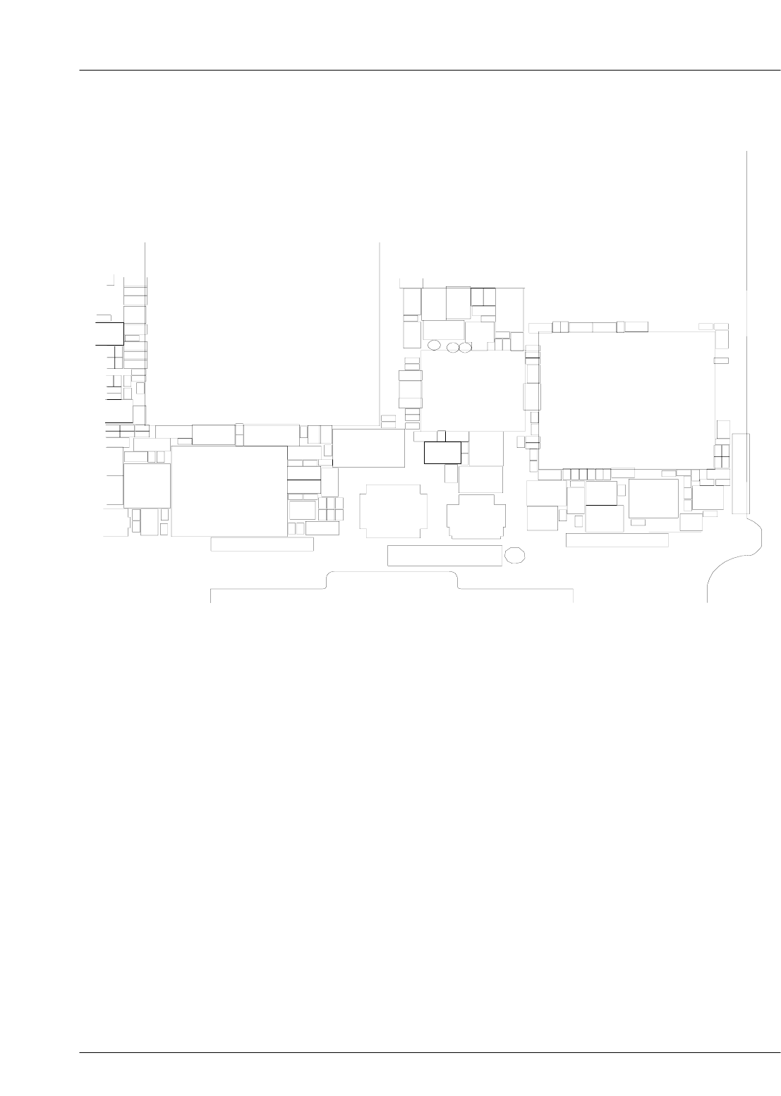
SAMSUNG Proprietary-Contents may change without notice
Flow Chart of Troubleshooting
10-11
This Document can not be used without Samsung’s authorization
C200
1
0
2
C
C202
3
0
2
C
4
0
2
C
5
0
2
C
C206C207
C208
9
0
2
C
C210
C211 C212
C213
C214
5
1
2
C
6
1
2
C
7
1
2
C
C218
9
1
2
C
0
2
2
C
1
2
2
C
2
2
2
C
3
2
2
C
7
2
2
C
8
2
2
C
3
3
2
C
4
3
2
C
5
3
2
C
C236
7
3
2
C
8
3
2
C
C239
C240
1
4
2
C
2
4
2
C
3
4
2
C
C244
5
4
2
C
6
4
2
C
C310
2
1
3
C
C313
C314
C315
C317
8
1
3
C
C319
0
2
3
C
1
2
3
C
C
0
0
4
C
C401
2
0
4
C
3
0
4
C
C405 C406 C407
C408
C409
C413C414
C415
C416
C417
8
1
4
C9
1
4
C
0
2
4
C
1
2
4
C
C422
C423
4
2
4
C
5
2
4
C
C426
7
2
4
C
8
2
4
C
9
2
4
C
C461
C462
5
6
4
C
6
6
4
C
7
6
4
C
C468
C600
C601
C605
C607
C610
C611
C614
C620
7
2
6
C
C632
C633
8
3
6
C
0
4
6
C
C641
2
4
6
C
C643
6
4
6
C
C651
2
5
6
C
C678
C679
2
8
6
C
CN201
D300
DF_ALEDF_CLE
0
0
4
C
D
H
1
0
3
L
2
0
3
L
MGND
0
0
3
C
S
O
0
0
4
C
S
O
OSC600
OSC601
R200
2
0
2
R
6
0
2
R
R207
9
0
2
R
R210
R211
R212
R213
4
1
2
R
5
1
2
R
6
1
2
R
7
1
2
R
R218
9
1
2
R
R220
1
2
2
R
2
2
2
R
R304
2
1
3
R
3
0
4
R
4
0
4
R
7
0
4
R
8
0
4
R
R409
0
1
4
R
1
1
4
R
2
1
4
R
4
1
4
R
5
1
4
R
R425
R426
7
2
4
R
R600
R601
R602
R610
6
R
1
0
1
C
S
SC113
SC117
SLC50 1
TA40 0
TA40 1 TA402
3
0
4
A
T
4
0
4
A
T
5
0
4
A
T
TP_CBL_PWR_ N
0
0
6
R
T
U200
U201
2
0
2
U3
0
2
U
U204
5
0
2
U
U206
7
0
2
U
U300
U600
7
0
6
U
U610
UCD402
0
0
2
P
C
U
UCP600
UME201
ZD40 0
ZD40 1
2
0
4
D
Z
ZD40 6
SAMSUNG Proprietary-Contents may change without notice
Flow Chart of Troubleshooting
10-12
This Document can not be used without Samsung’s authorization
10-3. SPEAKER Working
7, 9 PininU407
Signal ON ??
Check PIN 6, 10 in U407,
C477, C478
Y18, V21 Pin in UCP
Signal ON?
Operator Speaker
SPK-Assy’s Breakdown?
Check PIN 5, 8 in UCD 402
Change SPK-Assy’s
No
No
No
Yes
No
No
Yes
Yes
12, 14 PininU402
Signal ON ?Check L404, L405
Yes
END

SAMSUNG Proprietary-Contents may change without notice
Flow Chart of Troubleshooting
10-13
This Document can not be used without Samsung’s authorization
14
VOM
12
VOP
F
E
R
V
19
S
S
V
8
13
VSS
S
S
V
18
D
D
V
9
11
VDD
15
VDD
17
D
D
V
1VIM1
2VIM2
3VIP1
4VIP2
21
D
N
G
1
S
G
6 7
2
S
G
C
N
2223
C
N
M
V
C
R
16
10
P
V
C
R
20
L
E
S
U402
5EN
C454
R432
R431
C459
VBATT
R433
R430
C443
L409
L410
C447
C448
VBATT
C442
C452
TA407
SPK_SW
RCV_P
RCV_N
AMP_EN_O
SPK_OUT_L
SPK_OUT_R
CODEC_OUT_R
CODEC_OUT_L
9
2
4
C
6
ZD402
1
2
34
5
VAUDIO_3.3V_A
5
6
4
C
0
0
4
A
T
C422
C402
C405
4
IO3
IO4 5
6
IO5
C424
ZD406
2GND
IO1
1
IO2
3
8
6
4
C
6
6
4
C
C403
C428
TA403
C417
TA405
C425
VMICBIAS_2.7V
7
6
4
C
C401
VCODEC_2.0V
VAUDIO_3.0V
5
1
4
R
4
1
4
R
VAUDIO_3.3V_A
R412
C407
TA401
VAUDIO_3.0V
C427
9
6
4
C
R411
0
0
4
C
OSC400
GND
2
3
OUT
4
VDD
1
_ST
C416
R410
8
0
4
C
R409
TA402
VAUDIO_3.3V_A
5
1
Y+
7
1
Y-
6
0
4
C
8
3
SPKVDD
0
1C
N
Y
S
8
1
TPGND
3
1
TPVDD
7
2
F
E
R
V
2
14
X
U
A
/
R
E
P
I
W
4
1
X+
6
1
X-
3
3
4
T
U
O
9
1
PCBEEP
1
17
O
I
P
G
/
B
T
E
S
E
R
8N
I
A
T
A
D
S
5T
U
O
A
T
A
D
S
4
3
D
N
G
K
P
S
5
3
L
K
P
S
6
3
R
K
P
S
0
3
2
X
U
A
/
2
P
M
O
C
/
B
2
C
I
M
8
2
S
A
I
B
C
I
M
2
2
MICOM
1
3
O
N
O
M
0
2
MONOIN
0
5
NC
1
5
NC
7
3
OUT3
1
4
HPR
HPVDD
3
4
3
2
LINEL
4
2
LINER
2A
K
L
C
M
3B
K
L
C
M
1
2
MIC1
9
2
1
X
U
A
/
1
P
M
O
C
/
A
2
C
I
M
GND
4
4
9
4
GPIO1/PCMCLK
5
4
GPIO2/IRQ
6
4
GPIO3/PENDOWN/PCMFS
7
4
GPIO4/ADA/MASK/PCMDAC
8
4
GPIO5/SPDIF/PCMADC
0
4
HPGND
9
3
HPL
2
4
AGND2
5
2
D
D
V
A
6K
L
C
T
I
B
2
3
2
P
A
C
1D
D
V
B
D
9D
D
V
C
D
41
D
N
G
D
72
D
N
G
D
UCD402
6
2
D
N
G
A
K
L
C
T
I
B
TSPX
TSPY
TSMX
TSMY
CODECCLK_EN
D
N
G
_
C
C
V
_
J
O
RADIO_L
RADIO_R
MSM_SPK_N
P
_
C
I
M
_
M
S
M
EARCOM
T
U
O
_
A
T
A
D
S
C
N
Y
S
SPKL
SPKR
BT_PCM_SYNC
T
S
R
_
7
9
C
A
n
BT_PCM_CLK
BT_PCM_OUT
BT_PCM_IN
EAROUT_L
EAROUT_R
SPK_SW
MSM_SPK_P
MSM_MIC_N
MIC_P
MIC_N
N
I
_
A
T
A
D
S
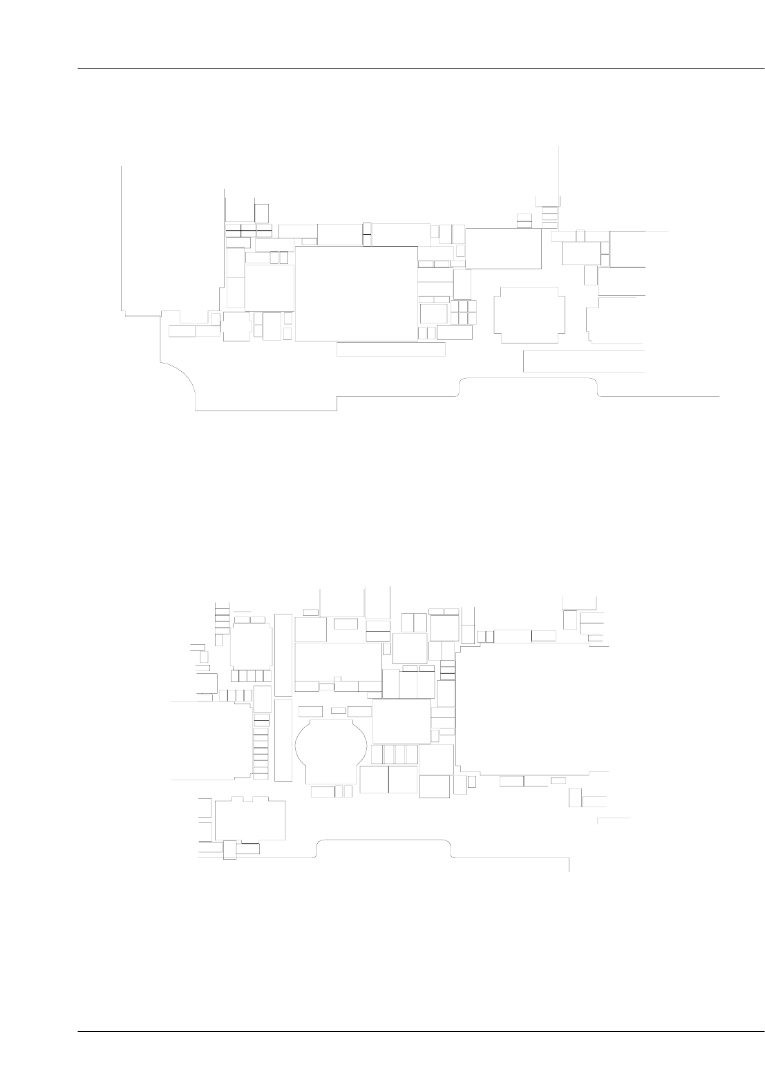
SAMSUNG Proprietary-Contents may change without notice
Flow Chart of Troubleshooting
10-14
This Document can not be used without Samsung’s authorization
4
3
2
C
5
3
2
C
C236
C240
2
4
2
C
5
4
2
C
C307
0
0
4
C
C401
2
0
4
C
3
0
4
C
C405 C406 C407
C408
C409
C413C414
C415
C416
C417
C422
4
2
4
C
5
2
4
C
7
2
4
C
8
2
4
C
9
2
4
C
C461
C462
5
6
4
C
6
6
4
C
7
6
4
C
C468
7
2
6
C
C633
8
3
6
C
0
4
6
C
C641
2
4
6
C
C643
6
4
6
C
CN201
0
0
4
C
D
H
0
0
4
C
F
I
0
0
4
C
S
O
OSC600
OSC601
R220
0
0
3
R
R409
0
1
4
R
1
1
4
R
2
1
4
R
4
1
4
R
5
1
4
R
R425
R426
7
2
4
R
R600
R601
SC117
SLC50 1
TA40 0
TA40 1TA402
3
0
4
A
T
4
0
4
A
T
5
0
4
A
T
5
0
2
U
U206
U30 0
UCD402
UME201
ZD30 0
ZD40 0
2
0
4
D
Z
ZD40 6
0
0
3
T
A
B
9
0
1
C
0
1
1
C
1
0
1
1
C
2
0
1
1
C
C110 4 C1105
6
0
1
1
C
7
0
1
1
C
8
0
1
1
C
9
0
1
1
C
1
1
1
C
C113
C114
C115
C116
7
1
1
C
C118
C121
C122
C130
C132
C133
7
3
1
C
8
3
1
C
C150
6
5
1
C
C196
C197
9
9
1
C
C323
0
1
4
C
C411
C412
C442
C443
7
4
4
C
8
4
4
C
C452 C454
5
5
4
C
6
5
4
C
C459
C469
3
0
5
C
4
0
5
C
C519
C527 C532
1
4
5
C
C546 C63 7
C680
0
0
1
F
0
0
1
L
L10 1
2
0
1
L
L11 9
4
2
1
L
9
0
4
L
0
1
4
L
4
0
2
0
1
C
S
O
PAM100
R100
R102
R103
R104
5
0
1
R
R106
R107
R108
R109
2
2
1
R
R123
R124
7
2
1
R
R129
5
3
1
R
R137
8
3
1
R
R139
R306
R430
1
3
4
R
2
3
4
R
R433
5
3
4
R
6
0
5
R
R507
R509
1
1
5
R
R512
8
1
5
R
R631
RFS100
2
0
1
C
S
9
0
1
C
S
TA10 0
7
0
4
A
T
U101
U401
U402
U407
7
0
5
U
1
1
8
0
6
U
VR50 0
ZD40 3ZD40 4
5
0
4
D
Z
SAMSUNG Proprietary-Contents may change without notice
Flow Chart of Troubleshooting
10-15
This Document can not be used without Samsung’s authorization
10-4. MIC Working
3,4Pin in
IFC400 Signal
ON?
3.5Pin in
HDC400
Signal ON?
Change Earphone
Check the DC bias voltage on MIC path
Change
MIC Assy’s
Yes
Check the path around MIC Bais circuit
The voltage of
R418 is about
1.6V ?
No
YES
No
Operate Microwave
Yes
Yes
No
AE17, AE18 in
UCP200 Signal
ON ?
YES
No
Check the C405, C406, UCD402
END
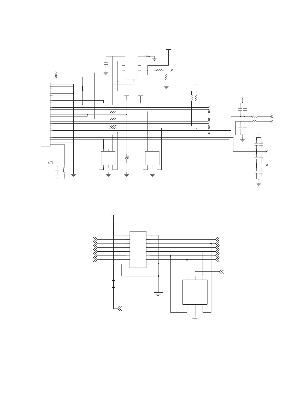
SAMSUNG Proprietary-Contents may change without notice
Flow Chart of Troubleshooting
10-16
This Document can not be used without Samsung’s authorization
9
0
4
C
6
5
H
C
2N
V
ZD400
11
H
C
2
H
C4
33
H
C
5
4
H
C
NC 21
22
NC
23
NC
NC 24
25
NC
NC 26
NC 27
33
4
4
55
6
6
77
8
8
99
14
14
15 15
16
16
17 17
18
18
19 19
2
2
20
20
IFC400
11
10
10
11 11
12
12
13
13
VUSB_5V
5
1
4
C
R404
VEXT_5V
R406
1
2
4
C
4
1
4
C
8
1
4
C
V_DC
9
1
4
C
2N
V
ZD401
11
H
C
2
H
C4
33
H
C
5
4
H
C
6
5
H
C
C453
VCC_3.0V
TA404
0
2
4
C
R407
R403
R428
6
7
OUT
_EN 10
_FLAG
3
GND
11
D
N
G
1IN
4IN
IN5
12
N
I
NC 8
9
NC
OUT
U409
2
R425
R401
R408
3
2
4
C
C470
L402
R402
3
1
4
C
6
2
4
C
R405
R426
RADIO_ANT
IF_CON_SENSE
EAR_CHECK
JTAG_VBUS
USB_DETECT
EAR_COM
D+
D-
EAR_MIC_P
EAR_MIC_N
EAROUT_R
EAROUT_L
SEND_END
nJACK_INT
RXD
TXD_TVOUT
JTAG_RXD
JTAG_IF_CON_SENSE
VCC_3.0V
5
H
C
2N
V
5
0
4
D
Z
11
H
C
2
H
C4
33
H
C
5
4
H
C
6
77 8
8
99
14
15
15 16 16
2
2
33 4
4
55 6
6
HDC400
11
10 10
1111 12
12
13
13 14
MOUSE_CLK
EAR_CHECK
MAIN_MIC_P
OJ_VCC_GND
MOUSE_TXD
MOUSE_nCS
MOUSE_SHDN
MOUSE_RXD
KBC(2)
MOUSE_MOTION
MAIN_MIC_N
KBR(1)
KBR(0)
KBR(2)
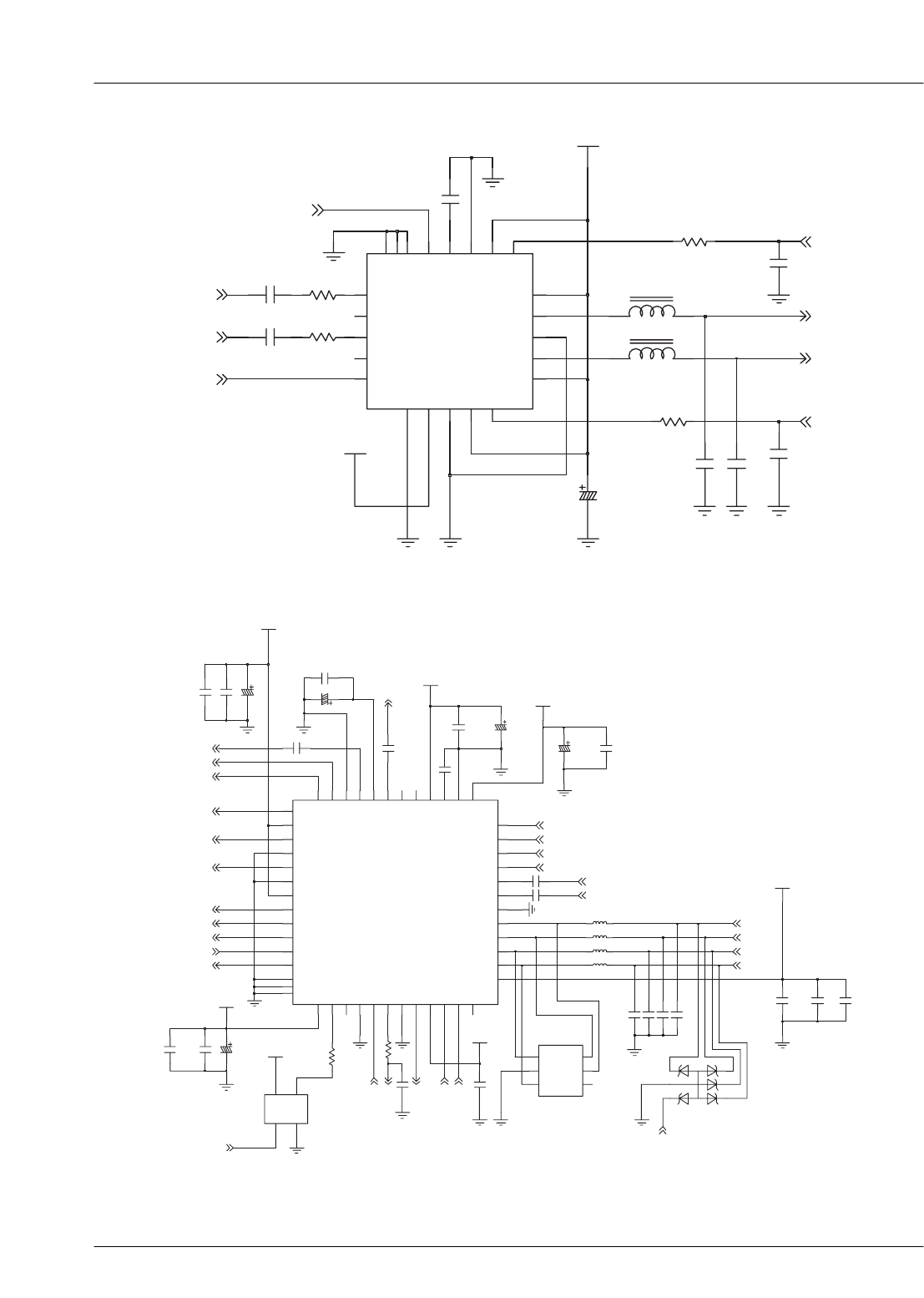
SAMSUNG Proprietary-Contents may change without notice
Flow Chart of Troubleshooting
10-17
This Document can not be used without Samsung’s authorization
14
VOM
12
VOP
F
E
R
V
19
S
S
V
8
13
VSS
S
S
V
18
D
D
V
9
11
VDD
15
VDD
17
D
D
V
1VIM1
2VIM2
3VIP1
4VIP2
21
D
N
G
1
S
G
6 7
2
S
G
C
N
2223
C
N
M
V
C
R
16
10
P
V
C
R
20
L
E
S
U402
5EN
C454
R432
R431
C459
VBATT
R433
R430
C443
L409
L410
C447
C448
VBATT
C442
C452
TA407
SPK_SW
RCV_P
RCV_N
AMP_EN_O
SPK_OUT_L
SPK_OUT_R
CODEC_OUT_R
CODEC_OUT_L
9
2
4
C
6
ZD402
1
2
34
5
VAUDIO_3.3V_A
5
6
4
C
0
0
4
A
T
C422
C402
C405
4
IO3
IO4 5
6
IO5
C424
ZD406
2GND
IO1
1
IO2
3
8
6
4
C
6
6
4
C
C403
C428
TA403
C417
TA405
C425
VMICBIAS_2.7V
7
6
4
C
C401
VCODEC_2.0V
VAUDIO_3.0V
5
1
4
R
4
1
4
R
VAUDIO_3.3V_A
R412
C407
TA401
VAUDIO_3.0V
C427
9
6
4
C
R411
0
0
4
C
OSC400
GND
2
3
OUT
4
VDD
1
_ST
C416
R410
8
0
4
C
R409
TA402
VAUDIO_3.3V_A
5
1
Y+
7
1
Y-
6
0
4
C
8
3
SPKVDD
0
1C
N
Y
S
8
1
TPGND
3
1
TPVDD
7
2
F
E
R
V
2
14
X
U
A/
R
E
PI
W
4
1
X+
6
1
X-
3
3
4
T
U
O
9
1
PCBEEP
1
17
OI
P
G/
B
T
E
S
E
R
8NI
A
T
A
D
S
5T
U
O
A
T
A
D
S
4
3
D
N
G
K
P
S
5
3
L
K
P
S
6
3
R
K
P
S
0
3
2
X
U
A
/
2
P
M
O
C
/
B
2
C
I
M
8
2
S
A
I
B
C
I
M
2
2
MICOM
1
3
O
N
O
M
0
2
MONOIN
0
5
NC
1
5
NC
7
3
OUT3
1
4
HPR
HPVDD
3
4
3
2
LINEL
4
2
LINER
2A
K
L
C
M
3B
K
L
C
M
1
2
MIC1
9
2
1
X
U
A
/
1
P
M
O
C
/
A
2
C
I
M
GND
4
4
9
4
GPIO1/PCMCLK
5
4
GPIO2/IRQ
6
4
GPIO3/PENDOWN/PCMFS
7
4
GPIO4/ADA/MASK/PCMDAC
8
4
GPIO5/SPDIF/PCMADC
0
4
HPGND
9
3
HPL
2
4
AGND2
5
2
D
D
V
A
6K
L
C
T
I
B
2
3
2
P
A
C
1D
D
V
B
D
9D
D
V
C
D
41
D
N
G
D
72
D
N
G
D
UCD402
6
2
D
N
G
A
K
L
C
T
I
B
TSPX
TSPY
TSMX
TSMY
CODECCLK_EN
D
N
G
_
C
C
V
_
J
O
RADIO_L
RADIO_R
MSM_SPK_N
P
_
C
I
M
_
M
S
M
EARCOM
T
U
O
_
A
T
A
D
S
C
N
Y
S
SPKL
SPKR
BT_PCM_SYNC
T
S
R
_
7
9
C
A
n
BT_PCM_CLK
BT_PCM_OUT
BT_PCM_IN
EAROUT_L
EAROUT_R
SPK_SW
MSM_SPK_P
MSM_MIC_N
MIC_P
MIC_N
N
I
_
A
T
A
D
S
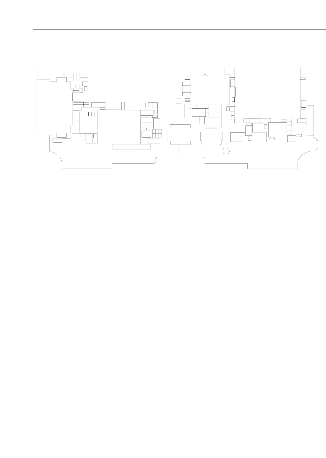
SAMSUNG Proprietary-Contents may change without notice
Flow Chart of Troubleshooting
10-18
This Document can not be used without Samsung’s authorization
C200
1
0
2
C
C202
3
0
2
C
4
0
2
C
C208
9
0
2
C
C210 C213
6
1
2
C
7
1
2
C
C218
9
1
2
C
0
2
2
C
1
2
2
C
2
2
2
C
3
2
2
C
C
4
3
2
C
5
3
2
C
C236
7
3
2
C
8
3
2
C
C239
C240
1
4
2
C
2
4
2
C
3
4
2
C
C244
5
4
2
C
6
4
2
C
C307
C
0
0
4
C
C401
2
0
4
C
3
0
4
C
C405 C406 C407
C408
C409
C413C414
C415
C416
C417
8
1
4
C9
1
4
C
0
2
4
C
1
2
4
C
C422
C423
4
2
4
C
5
2
4
C
C426
7
2
4
C
8
2
4
C
9
2
4
C
C461
C462
5
6
4
C
6
6
4
C
7
6
4
C
C468
C605
9
0
6
C
C610
C620
7
2
6
C
C632
C633
8
3
6
C
0
4
6
C
C641
2
4
6
C
C643
6
4
6
C
C651
2
5
6
C
C678
C679
2
8
6
C
CN201
0
0
4
C
D
H
0
0
4
C
F
I
MGND
0
0
4
C
S
O
OSC600
OSC601
R200
2
0
2
R
6
0
2
R
9
0
2
R
R210
R211
R212
R213
4
1
2
R
5
1
2
R
6
1
2
R
7
1
2
R
R218
R220
1
2
2
R
2
2
2
R
0
0
3
R
R304
0
4
R
0
4
R
R405
7
0
4
R
8
0
4
R
R409
0
1
4
R
1
1
4
R
2
1
4
R
4
1
4
R
5
1
4
R
R425
R426
7
2
4
R
R600
R601
R602
R610
1
0
1
C
S
SC113
SC117
SLC50 1
TA40 0
TA40 1TA402
3
0
4
A
T
4
0
4
A
T
5
0
4
A
T
TA60 0
0
0
6
R
T
U200
U201
2
0
2
U
3
0
2
U
U204
5
0
2
U
U206
7
0
2
U
U300
7
0
6
U
U610
UCD402
0
0
2
P
C
U
UME201
ZD300
ZD40 0
2
0
4
D
Z
ZD40 6
SAMSUNG Proprietary-Contents may change without notice
Flow Chart of Troubleshooting
10-19
This Document can not be used without Samsung’s authorization
10-5. KEY Working
Press Key
Yes
Yes
Yes
Yes
Yes
YES No
END
Change Key FPCB
Change OJ Key
Key FPCB
Breakdown? Change Key FPCB
Yes
Camera Key
FPCB
Breakdown?
Volume Key
NG ?
No
Camera Key
NG ?
Yes
No
OJ key NG?
Yes
No
OJ Key
Breakdown?
Power Key NG?
Change LED
Change Key FPCB
Key FPCB Breakdown?
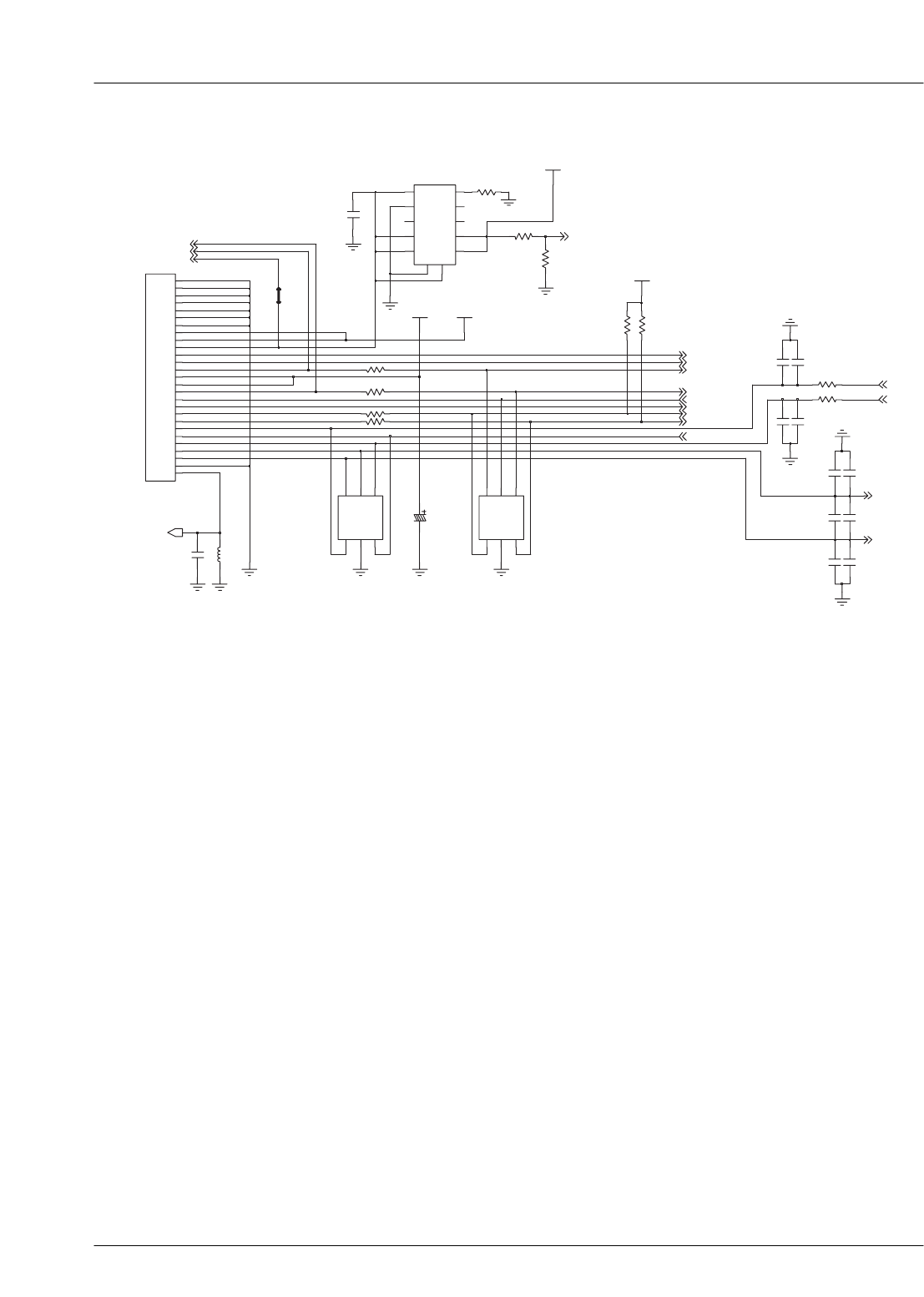
SAMSUNG Proprietary-Contents may change without notice
Flow Chart of Troubleshooting
10-20
This Document can not be used without Samsung’s authorization
9
0
4
C
6
5
H
C
2N
V
ZD400
11
H
C
2
H
C4
33
H
C
5
4
H
C
NC 21
22
NC
23
NC
NC 24
25
NC
NC 26
NC 27
33
4
4
55
6
6
77
8
8
99
14
14
15 15
16
16
17 17
18
18
19 19
2
2
20
20
IFC400
11
10
10
11 11
12
12
13
13
VUSB_5V
5
1
4
C
R404
VEXT_5V
R406
1
2
4
C
4
1
4
C
8
1
4
C
V_DC
9
1
4
C
2N
V
ZD401
11
H
C
2
H
C4
33
H
C
5
4
H
C
6
5
H
C
C453
VCC_3.0V
TA404
0
2
4
C
R407
R403
R428
6
7
OUT
_EN 10
_FLAG
3
GND
11
D
N
G
1IN
4IN
IN5
12
N
I
NC 8
9
NC
OUT
U409
2
R425
R401
R408
3
2
4
C
C470
L402
R402
3
1
4
C
6
2
4
C
R405
R426
RADIO_ANT
IF_CON_SENSE
EAR_CHECK
JTAG_VBUS
USB_DETECT
EAR_COM
D+
D-
EAR_MIC_P
EAR_MIC_N
EAROUT_R
EAROUT_L
SEND_END
nJACK_INT
RXD
TXD_TVOUT
JTAG_RXD
JTAG_IF_CON_SENSE
SAMSUNG Proprietary-Contents may change without notice
Flow Chart of Troubleshooting
10-21
This Document can not be used without Samsung’s authorization
10-6. T-Flash Card Working
Insert T-Flash
NG
C547
D
N
G
9
NC
45
NC
VDD 7
8
VOUT1
6
VOUT2
U508
CE1
1
3CE2
2GND
C530
VLCD_3.0V VTF_3.0VVBATT
LCD_EN
TF_EN
CN301
Breakdown?
Pin 1,2 in
CN301 short?
Yes
Change CN301
No
No
Change CN301
Yes
Change U508
Yes
No
Pin 2 in U508
Low?
Check U508 &Neighboring circuit
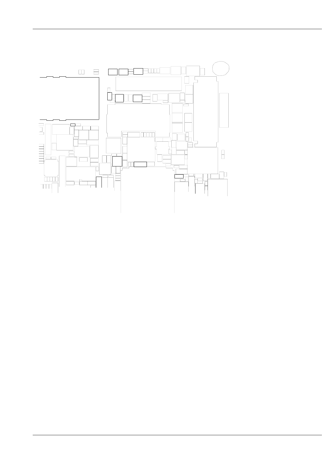
SAMSUNG Proprietary-Contents may change without notice
Flow Chart of Troubleshooting
10-22
This Document can not be used without Samsung’s authorization
BOTHHOLE6
0
2
0
1
C
C105
C107
C108
1
C
1
0
1
1
C
2
0
1
1
C
C1104 C1105
6
0
1
1
C
7
0
1
1
C
8
0
1
1
C
9
0
1
1
C
C1112
C115
C116
C130
C132
C133
1
C
1
C
1
C
C187
C197
9
9
1
C
C328
9
2
3
C
0
3
3
C
0
1
4
C
C411
C412
C442
4
4
4
C
C452 C454
0
7
4
C
C500
3
0
5
C
4
0
5
C
5
0
5
C
6
0
5
C
7
0
5
C
8
0
5
C
9
0
5
C
C510
C511
C512
3
1
5
C
C517
C518
C519
C520
C521
3
2
5
C
C524
5
2
5
C
C526
C527
0
3
5
C
C531
C532
3
3
5
C4
3
5
C
C535
C537C538
C540
1
4
5
C
2
4
5
C3
4
5
C
4
4
5
C
C546
7
4
5
C
C548
C549
C634
C635
C636
C637
C644
5
4
6
C
7
4
6
C
C649
0
5
6
C
9
5
6
C
8
5
6
C
C660
1
6
6
C
C662
C680
1
8
6
C
CN301
1
0
6
N
C
0
0
5
F
1
0
5
F2
0
5
F
3
0
5
F
F504
F505
0
0
5
C
D
H
1
0
5
C
D
H
2
1
L
L402
4
0
4
L
5
0
4
L
9
0
4
L
0
1
4
L
0
0
5
L
L501
L502L503
4
0
5
L
0
0
6
L
L601
OSC100
2
0
1
C
S
O
R101
1
R
R123
R124
7
2
1
R
R129
5
3
1
R
8
3
1
R
R317
9
1
3
R
0
2
3
R
1
2
3
R
2
2
3
R
3
2
3
R
R400
R
0
2
4
R
R423
R430
0
0
5
R
1
0
5
R
2
0
5
R
R507
R508
R509
R510
R512
R513
R514
R515
7
1
5
R
8
1
5
R
9
1
5
R
0
2
5
R
R604
6
0
6
R
8
0
6
R
7
0
6
R
R631
7
0
1
C
S
9
0
1
C
S
SIM300
TA100
7
0
4
A
T
0
0
5
R
T
1
0
5
R
T
2
0
5
R
T
U101
U306
U308
2
1
3
U
U401
4
U
U500
2
0
5
U
U503
U504
U505
U506
7
0
5
U
8
0
5
U
U509
U510
1
1
5
U
U512
4
1
5
U
U515
U516
1
0
6
U
8
0
6
U
U609
4
0
6
D
C
U
0
0
5
D
Z
ZD501
SAMSUNG Proprietary-Contents may change without notice
Flow Chart of Troubleshooting
10-23
This Document can not be used without Samsung’s authorization
10-7. Bluetooth Working
Ant103 and
L119 O.K?
No
Yes
Replace or Resolder Ant103 and L119
Change U101
Yes
No
Pin 6 in U101=3.3V
Pin5 in U101=1.8V
While trying to
operate BT
Replace MOD100
Operate BT
7
1VIN 6VOUT1
VOUT2
5
U101
4
EN1
EN2
3
GND
2
GND
VCOMBO_3.3V VCOMBO_1.8V
C1102C1101
VBATT
C199
COMBO_EN
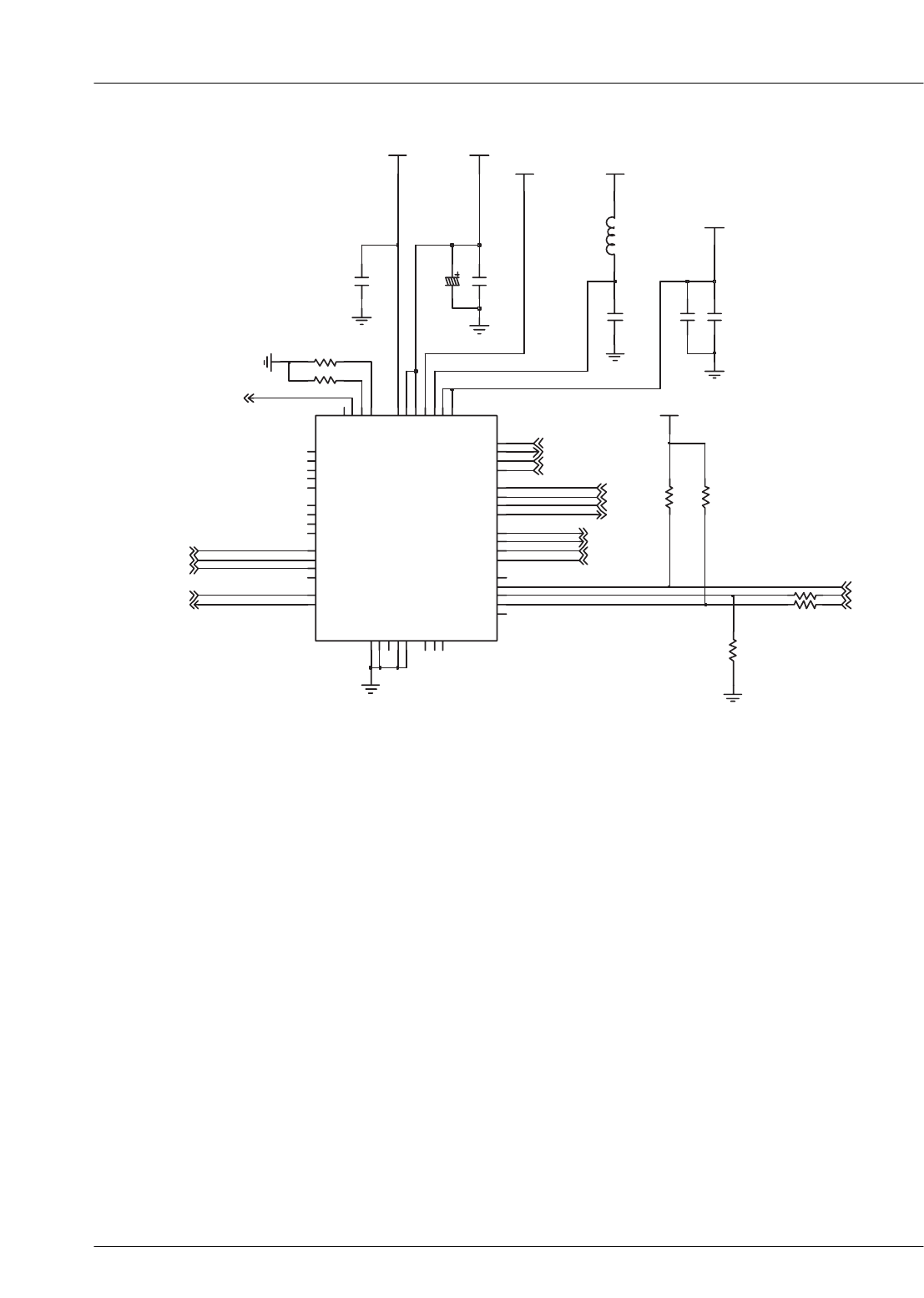
SAMSUNG Proprietary-Contents may change without notice
Flow Chart of Troubleshooting
10-24
This Document can not be used without Samsung’s authorization
7
9
1
C
L124
R138
4
9
1
C
VCC_3.0V
8
9
1
C
R124
5
W
_
D
8
.
1
D
D
V
0
5C
N
1
5C
N
6GPIO0
PIO2
7
8PIO3
9PIO0
2
4
W
_
O
I
D
D
V
3
4
W
_
3
.
3
D
D
V4
4
W
_
3
.
3
D
D
V
45
SLEEP_CLK_W
46 GPIO1
47
RESET_N_W
PDN 48
9
4C
N
5
3
36 SD_D3
37 SD_D2
38 SD_D1
39 SD_D0
4
W
_
A
8
.
1
D
D
V
SD_CMD
40
41 SD_CLK
XTAL_OUT_B
29
XTAL_IN_B
3
P
_
L
E
S
T
N
A
30
XTAL_IN_W
31
XTAL_OUT_W
32 GPIO5
33 GPIO6
34
TDO
D
N
G
PCM_CLK
21
UART_TX
22
UART_CTS
23
UART_RX
24
UART_RTS
5
2D
N
G
6
2
B
_
O
I
D
D
V
7
2
B
_
3
.
3
D
D
V
28
3
1D
N
G
14 PIO4
15 PIO1
16
RST_N_B
17
PCM_OUT 18
PCM_SYNC
19
PCM_IN
2
N
_
L
E
S
T
N
A
20
MOD100
1D
N
G
0
1
T
B
_
T
N
A
1
1D
N
G
2
1
T
B
|
N
A
L
W
_
T
N
A
VCC_3.0V
R123
6
9
1
C
VCOMBO_1.8V
VCOMBO_3.3V
R129 R127
VCOMBO_1.8V
5
9
1
C
0
0
1
A
T
R139
R137
VCOMBO_3.3V
WLAN_SPI_TXD
WLAN_SPI_nINT
WLAN_SPI_RXD
WLAN_SPI_nCS
WLAN_SPI_CLK
XTAL_OUT_W
XTAL_OUT_B
WLAN_nRST
BT_RTS
BT_CTS
BT_nRST
WLAN_PDN
COMBO_ANT
BT_TXD
BT_RXD
BT_PCM_CLK
BT_PCM_SYNC
BT_PCM_IN
BT_PCM_OUT
XTAL_IN_B
XTAL_IN_W
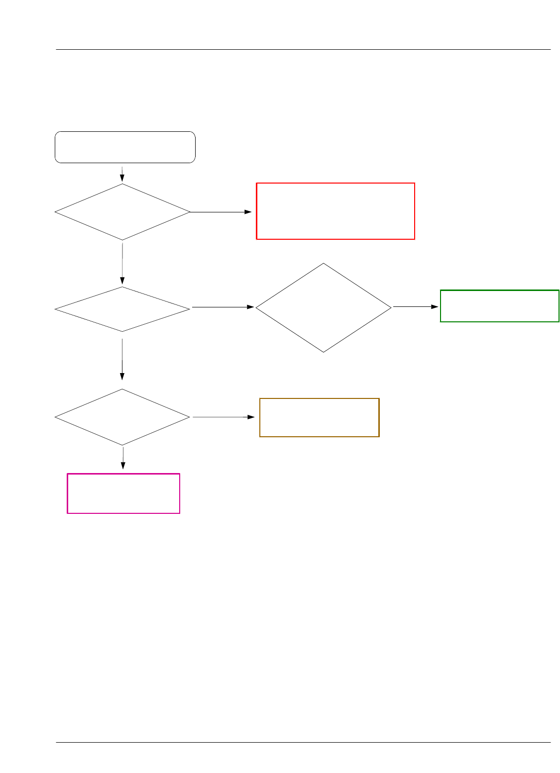
SAMSUNG Proprietary-Contents may change without notice
Flow Chart of Troubleshooting
10-25
This Document can not be used without Samsung’s authorization
10-8. GSM850 Receiver
RX ON
Sector PWR=-50dBm
Resolder or change
F100,L102,L103,C122
Change U100 &UCP200
PAM100 Pin 8
>= -60dBm
Check PAM100
Truth Table
Pin 1:HIGH
Pin 27 : LOW
Pin 28 : HIGH
No
Yes
Resolder RFS100, C103, R100, L100,
,L101, C111
Resolder or change PAM100
No
PAM100 Pin 4
>= -70dBm
Yes
U100
Pin 50,51
>= -75dBm
No
Yes
Yes
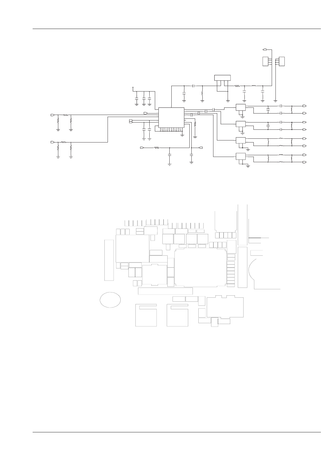
SAMSUNG Proprietary-Contents may change without notice
Flow Chart of Troubleshooting
10-26
This Document can not be used without Samsung’s authorization
11
2
23
34
4
R106
ANT100
C110
L105
C112
C155
R102
G
5
G
1IN
3
OUT
OUT 4
F100
2
C121
C138
C114
1
3
OUT
OUT 4
F101
G
2
G
5
IN
L104
L101
C137
G
2
G
5
1IN
OUT 3
OUT 4
F103 L109
C156
R100
C118 L103
C109
44
ANT101
1
1
22
33
G
2 5
G
1IN
OUT 3
4
OUT
F102
C131
L111
V_DC
L107
RX2
6
7
RX1
8
T
N
A
D
N
G
9
C135
25
VAPC
VBATT
26
BS2
27
28 BS1
GND29
3
RSVD
4
RX4
RX3
5
8
1D
N
G
9
1
D
N
G
2
MODE
D
N
G
0
2
21 DCS|PCS_IN
D
N
G
2
2
23
GSM_IN
D
N
G
4
2
10
WCDMA1
1
1D
N
G
D
N
G
2
1
D
N
G
3
1
D
N
G
4
1
D
N
G
5
1
6
1
D
N
G
7
1
D
N
G
PAM100
_TXEN 1
RFS100
2A
3C
1G
4G
R104
C122
L108
L102
C103
C136
L106
L100
R105
R107
L112
C145
C111
R103
R108
C120
C119
C150
R109
C113
N
TRX_WCDMA2100
PCS_RXM
GSM_RXP
GSM_RXM
GSM850_RXM
GSM850_RXP
PAM_RAMP+
GSM_ANT_SEL2_N
GSM_ANT_SEL1_N
DCS_RXP
DCS_RXM
PCS_RXP
RFOUT_DCS_PCS
RFOUT_GCELL_EGSM
GSM_ANT_SEL0_N
0
0
1
T
N
A
1
0
1
T
N
A
BOTHHOLE60 1 C10 3
9
0
1
C
0
1
1
C
6
0
1
1
C
7
0
1
1
C
8
0
1
1
C
9
0
1
1
C
1
1
1
C
0
1
1
1
C
1
1
1
1
C
3
1
4
1
C11 2
C113
C114
C118C119C120
C121
1
3
1
C
C135
7
3
1
C
8
3
1
C
4
4
C14 5
6
4
7
4
8
4
1
9
4
1
C150
C151
3
5
1
4
5
1
C15 5
6
5
1
C
5
6
1
C168
9
6
1
C
C17 0
4
7
1
C
9
7
1
C
0
8
1
C
C181
2
8
1
C
3
8
1
C
4
8
1
C
C51 9
0
0
1
P
U
D
0
0
1
F
1
0
1
F
2
0
1
F
3
0
1
F
F10 5
0
0
1
L
L10 1
2
0
1
L
3
0
1
L
4
0
1
L
5
0
1
L
6
0
1
L
7
0
1
L
9
0
1
L
1
1
1
L5
1
1
L
L11 6
6
2
1
L
2
0
1
PAM100
PAM101
R10 0
R102
R103
R104
5
0
1
R
R106
R107
R108
R109
6
1
1
R
R117
R118
5
3
1
R
R30 6
RFS10 0
2
0
1
C
S
4
0
1
C
S
9
0
1
SC11 6
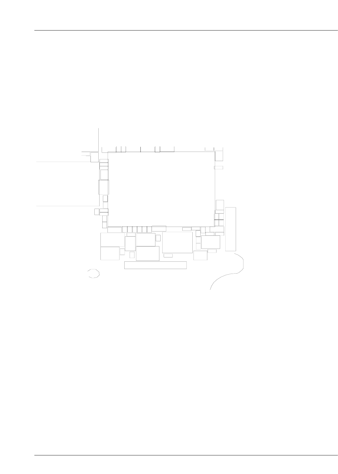
SAMSUNG Proprietary-Contents may change without notice
Flow Chart of Troubleshooting
10-27
This Document can not be used without Samsung’s authorization
C20 0
1
0
2
C
C202
3
0
2
C
4
0
2
C
5
0
2
C
C206C207
C20 8
9
0
2
C
C210
C21 1 C21 2
C21 3
C21 4
2
C
6
1
2
C
7
1
2
C
C218
9
1
2
C
0
2
2
C
1
2
2
C
2
2
2
C
3
2
2
C
2
C
2
C
3
3
2
C
7
3
2
C
8
3
2
C
1
4
2
C
3
4
2
C
C244
6
4
2
C
C317
C678
C679
2
8
6
C
MGND
O
R200
2
0
2
R
6
0
2
R
R20 7
9
0
2
R
R210
R211
R212
R213
4
1
2
R
5
1
2
R
6
1
2
R
7
1
2
R
R218
9
1
2
R
1
2
2
R
2
2
2
R
R304
1
0
1
C
S
SC11 3
0
0
6
R
T
U200
U201
2
0
2
U
3
0
2
U
7
0
2
U
7
0
6
U
U61 0
0
0
2
P
C
U
UME201
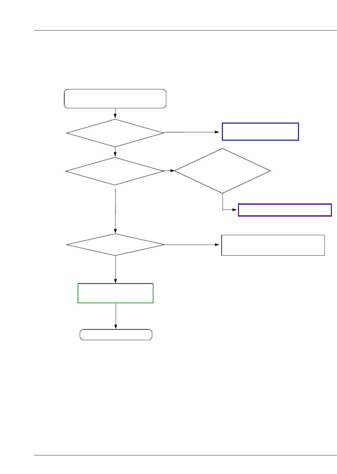
SAMSUNG Proprietary-Contents may change without notice
Flow Chart of Troubleshooting
10-28
This Document can not be used without Samsung’s authorization
10-9. GSM850 Transmitter
TX ON
(PCL 5level)
PAM100 Pin 23
>= 5dBm
U100 Pin 55
>= 5dBm
END
Resolder RFS100, C103, R100
,L100 ,L101, C111
Resolder or change PAM100
PAM100 Pin 8
>= 5dBm
Check PAM100
Truth Table
Pin 1:LOW
Pin 27 : HIGH
Pin 28 : LOW
No
No
No
Yes
Yes
Yes
YES
Resolder or change PAM100, C116, R106
,R108, R109
Check U100 &UCP200
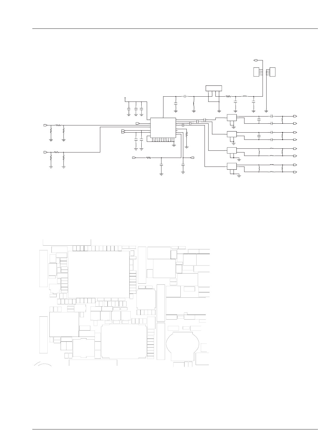
SAMSUNG Proprietary-Contents may change without notice
Flow Chart of Troubleshooting
10-29
This Document can not be used without Samsung’s authorization
0
0
3
T
A
B
0
0
1
C
1
0
1
C
2
0
1
C
C105
6
0
1
C
C107
C108
9
0
1
C
C110 4 C1105
6
0
1
1
C
7
0
1
1
C
8
0
1
1
C
9
0
1
1
C
0
1
1
1
C
1
1
1
1
C
C1112
3
1
1
1
C
4
1
1
1
C
C113
C114
C115
C116
7
1
1
C
C118C119C120
C121
C122
3
2
1
C
4
2
1
C
C125
6
2
1
C
7
2
1
C
8
2
1
C
9
2
1
C
C130
1
3
1
C
C132
C133
4
3
1
C
C135
C136
7
3
1
C
8
3
1
C
9
3
1
C
0
4
1
C
1
4
1
C
2
4
1
C
3
4
1
C
4
4
1
C
C14 5
6
4
1
C
7
4
1
C
8
4
1
C
9
4
1
C
C150
C151
C152
3
5
1
C
4
5
1
C
C15 5
6
5
1
C
C157
C159
C160
C161
C162
3
6
1
C
5
6
1
C
4
6
1
C
C166
C167
C168
9
6
1
C
C17 0
C171
C172
C173
4
7
1
C
6
7
1
C
C177
8
7
1
C
9
7
1
C
0
8
1
C
C181
2
8
1
C
3
8
1
C
4
8
1
C
C190
C323
C328
C41 1
C41 2
C442
7
4
4
C
C45 9
C51 9
3
2
5
C
C524
5
2
5
C
3
3
5
C4
3
5
C
C535
C53 7C53 8
C54 0
C54 6
C54 9
C680
0
0
1
P
U
D
0
0
1
F
1
0
1
F
2
0
1
F
3
0
1
F
4
0
1
F
F10 5
2
0
1
L
3
0
1
L
4
0
1
L
5
0
1
L
6
0
1
L
7
0
1
L
L108
9
0
1
L
0
1
1
L
1
1
1
L
L112
4
1
1
L
5
1
1
L
L11 6
6
2
1
L
L501
4
0
5
L
2
0
1
C
S
O
PAM100
PAM101
R101
R102
R103
R104
5
0
1
R
R106
R107
R108
R109
0
1
1
R
R11 1
R11 2
6
1
1
R
R117
R118
5
3
1
R
R30 6
R43 0
0
5
R
R50 9
1
5
R
R512
R513
2
0
1
C
S
SC10 3
4
0
1
C
S
7
0
1
C
S
9
0
1
C
S
0
1
1
C
S
SC11 6
U100
U306
U506
7
0
5
U
U50 9
1
1
5
U
U51 2
8
0
6
U
VR50 0
ZD40 4
11
2
23
34
4
R106
ANT100
C110
L105
C112
C155
R102
G
5
G
1IN
3
OUT
OUT 4
F100
2
C121
C138
C114
1
3
OUT
OUT 4
F101
G
2
G
5
IN
L104
L101
C137
G
2
G
5
1IN
OUT 3
OUT 4
F103 L109
C156
R100
C118 L103
C109
44
ANT101
1
1
22
33
G
2 5
G
1IN
OUT 3
4
OUT
F102
C131
L111
V_DC
L107
RX2
6
7
RX1
8
T
N
A
D
N
G
9
C135
25
VAPC
VBATT
26
BS2
27
28 BS1
GND29
3
RSVD
4
RX4
RX3
5
8
1D
N
G
9
1
D
N
G
2
MODE
D
N
G
0
2
21 DCS|PCS_IN
D
N
G
2
2
23
GSM_IN
D
N
G
4
2
10
WCDMA1
1
1D
N
G
D
N
G
2
1
D
N
G
3
1
D
N
G
4
1
D
N
G
5
1
6
1
D
N
G
7
1
D
N
G
PAM100
_TXEN 1
RFS100
2A
3C
1G
4G
R104
C122
L108
L102
C103
C136
L106
L100
R105
R107
L112
C145
C111
R103
R108
C120
C119
C150
R109
C113
T
TRX_WCDMA2100
PCS_RXM
GSM_RXP
GSM_RXM
GSM850_RXM
GSM850_RXP
PAM_RAMP+
GSM_ANT_SEL2_N
GSM_ANT_SEL1_N
DCS_RXP
DCS_RXM
PCS_RXP
RFOUT_DCS_PCS
RFOUT_GCELL_EGSM
GSM_ANT_SEL0_N
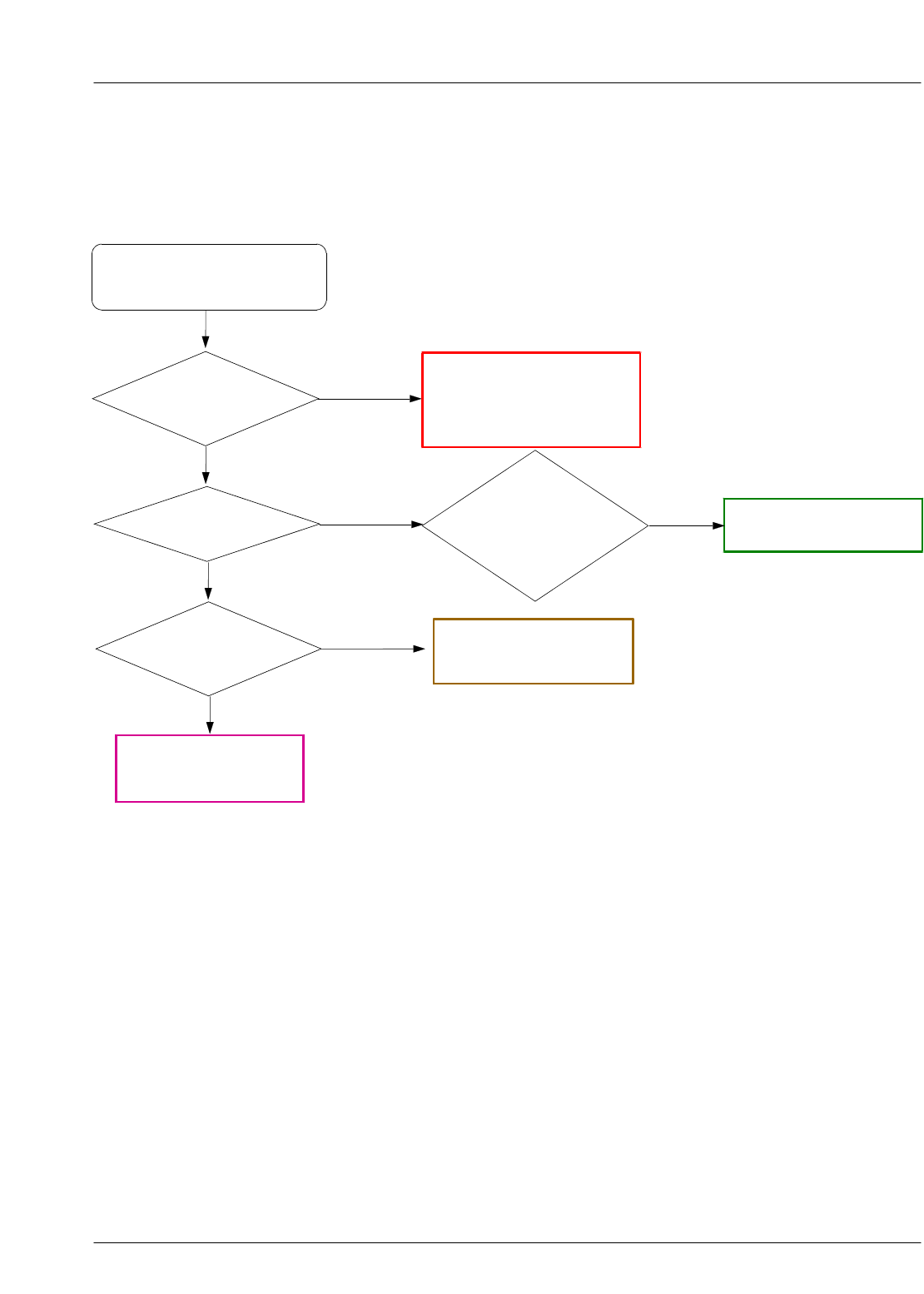
SAMSUNG Proprietary-Contents may change without notice
Flow Chart of Troubleshooting
10-30
This Document can not be used without Samsung’s authorization
10-10. GSM900 Receiver
RX ON
Sector PWR=50dBm
Resolder or change F101
,L104, L105, C136
Change U100 &UCP200
PAM100 Pin8
>= -60dBm
Check PAM100
Truth Table
Pin 1:HIGH
Pin 27 : HIGH
Pin 28 : HIGH
No
Yes
Resolder RFS100, C103, R100
,L100 ,L101, C111
Resolder or change PAM100
No
F100 Pin 5
>= -70dBm
Yes
U100 Pin 48,49
>= -75dBm
No
Yes
Yes
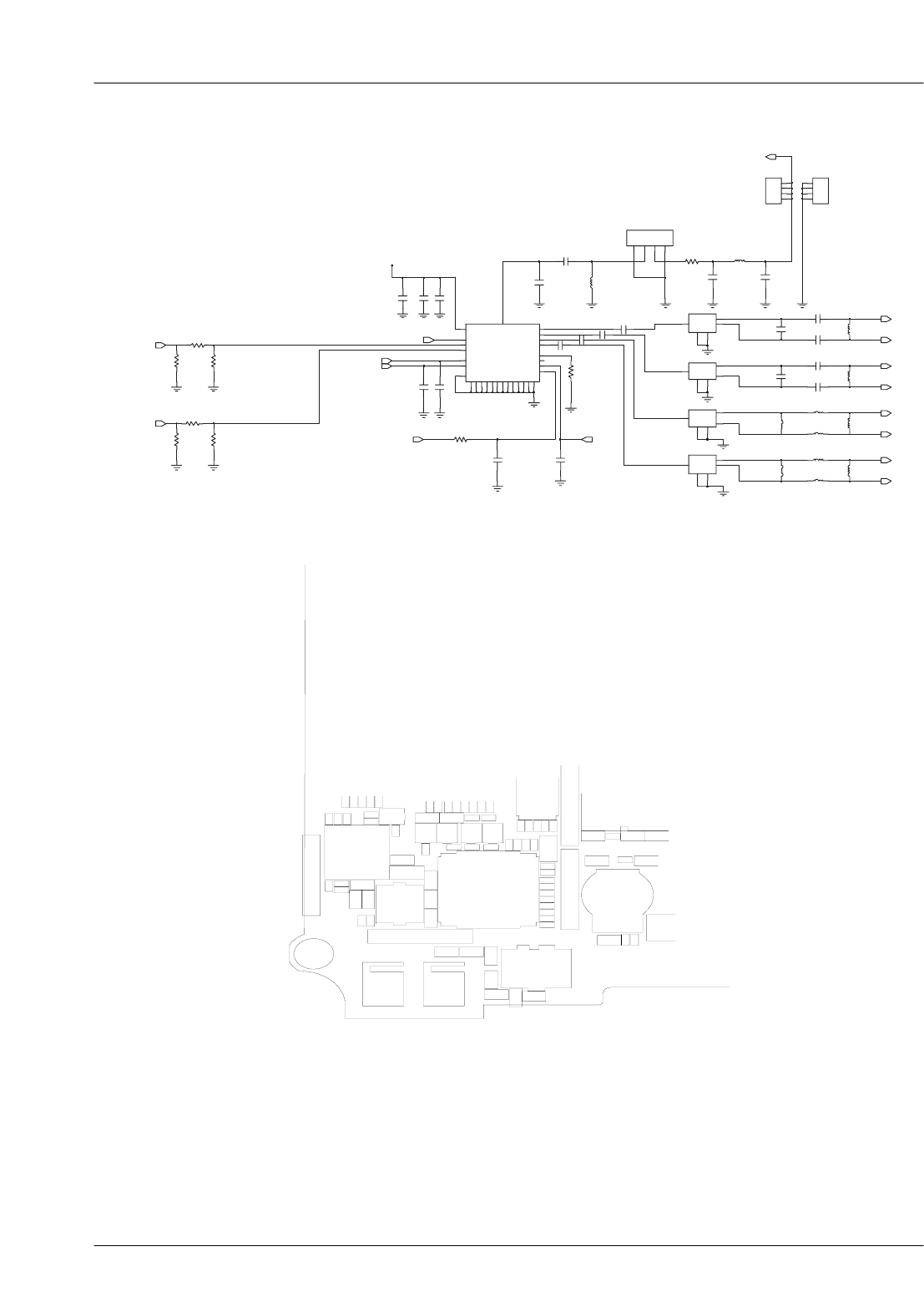
SAMSUNG Proprietary-Contents may change without notice
Flow Chart of Troubleshooting
10-31
This Document can not be used without Samsung’s authorization
0
0
1
T
N
A
1
0
1
T
N
A
0
0
3
T
A
B
BOTHHOLE601 C10 3
9
0
1
C
0
1
1
C
6
0
1
1
C
7
0
1
1
C
8
0
1
1
C
9
0
1
1
C
1
1
1
C
0
1
1
1
C
1
1
1
1
C
C11 2
C113
C114
C118C119C120
C121
1
3
1
C
C135
7
3
1
C
8
3
1
C
C14 5
8
9
C150
C151
3
4
C15 5
6
5
1
C
5
C168
9
6
1
C
C17 0
4
7
1
C
9
7
1
C
0
8
1
C
C181
2
8
1
C
3
8
1
C
4
8
1
C
C323 C45 9
C51 9
0
0
1
P
U
D
0
0
1
F
1
0
1
F
2
0
1
F
3
0
1
F
F10 5
0
0
1
L
L10 1
2
0
1
3
0
1
4
0
1
5
0
1
6
0
1
7
0
1
9
0
1
1
1
1
5
1
1
L
L11 6
6
2
1
L
2
0
PAM100
PAM101
R10 0
R102
R103
R104
5
0
1
R
R106
R107
R108
R109
6
1
1
R
R117
R118
5
3
1
R
R30 6
R43 0
6
0
5
R
R50 9
1
1
5
R
R512
RFS10 0
2
0
1
C
S
4
0
1
C
S
9
0
1
SC11 6
7
0
5
VR50 0
ZD40 4
11
2
23
34
4
R106
ANT100
C110
L105
C112
C155
R102
G
5
G
1IN
3
OUT
OUT 4
F100
2
C121
C138
C114
1
3
OUT
OUT 4
F101
G
2
G
5
IN
L104
L101
C137
G
2
G
5
1IN
OUT 3
OUT 4
F103 L109
C156
R100
C118 L103
C109
44
ANT101
1
1
22
33
G
2 5
G
1IN
OUT 3
4
OUT
F102
C131
L111
V_DC
L107
RX2
6
7
RX1
8
T
N
A
D
N
G
9
C135
25
VAPC
VBATT
26
BS2
27
28 BS1
GND29
3
RSVD
4
RX4
RX3
5
8
1D
N
G
9
1
D
N
G
2
MODE
D
N
G
0
2
21 DCS|PCS_IN
D
N
G
2
2
23
GSM_IN
D
N
G
4
2
10
WCDMA1
1
1D
N
G
D
N
G
2
1
D
N
G
3
1
D
N
G
4
1
D
N
G
5
1
6
1
D
N
G
7
1
D
N
G
PAM100
_TXEN 1
RFS100
2A
3C
1G
4G
R104
C122
L108
L102
C103
C136
L106
L100
R105
R107
L112
C145
C111
R103
R108
C120
C119
C150
R109
C113
TRX_WCDMA2100
PCS_RXM
GSM_RXP
GSM_RXM
GSM850_RXM
GSM850_RXP
PAM_RAMP+
GSM_ANT_SEL2_N
GSM_ANT_SEL1_N
DCS_RXP
DCS_RXM
PCS_RXP
RFOUT_DCS_PCS
RFOUT_GCELL_EGSM
GSM_ANT_SEL0_N
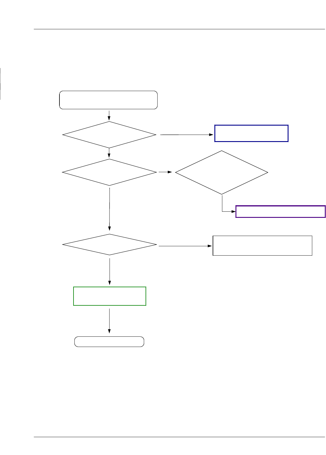
SAMSUNG Proprietary-Contents may change without notice
Flow Chart of Troubleshooting
10-32
This Document can not be used without Samsung’s authorization
10-9. GSM900 Transmitter
TX ON
(PCL 5level)
PAM100 Pin 23>=5dBm
U100 Pin 55>=5dBm
END
Resolder RFS100, C103, R100
,L100 ,L101, C111
Resolder or change PAM100
PAM100 Pin 8>=5
dBm
Check PAM100
Truth Table
Pin 1:LOW
Pin 27 : HIGH
Pin 28 : LOW
No
No
No
Yes
Yes
Yes
YES
Resolder or change PAM100, C116, R106
,R108, R109
Check U100 &UCP200
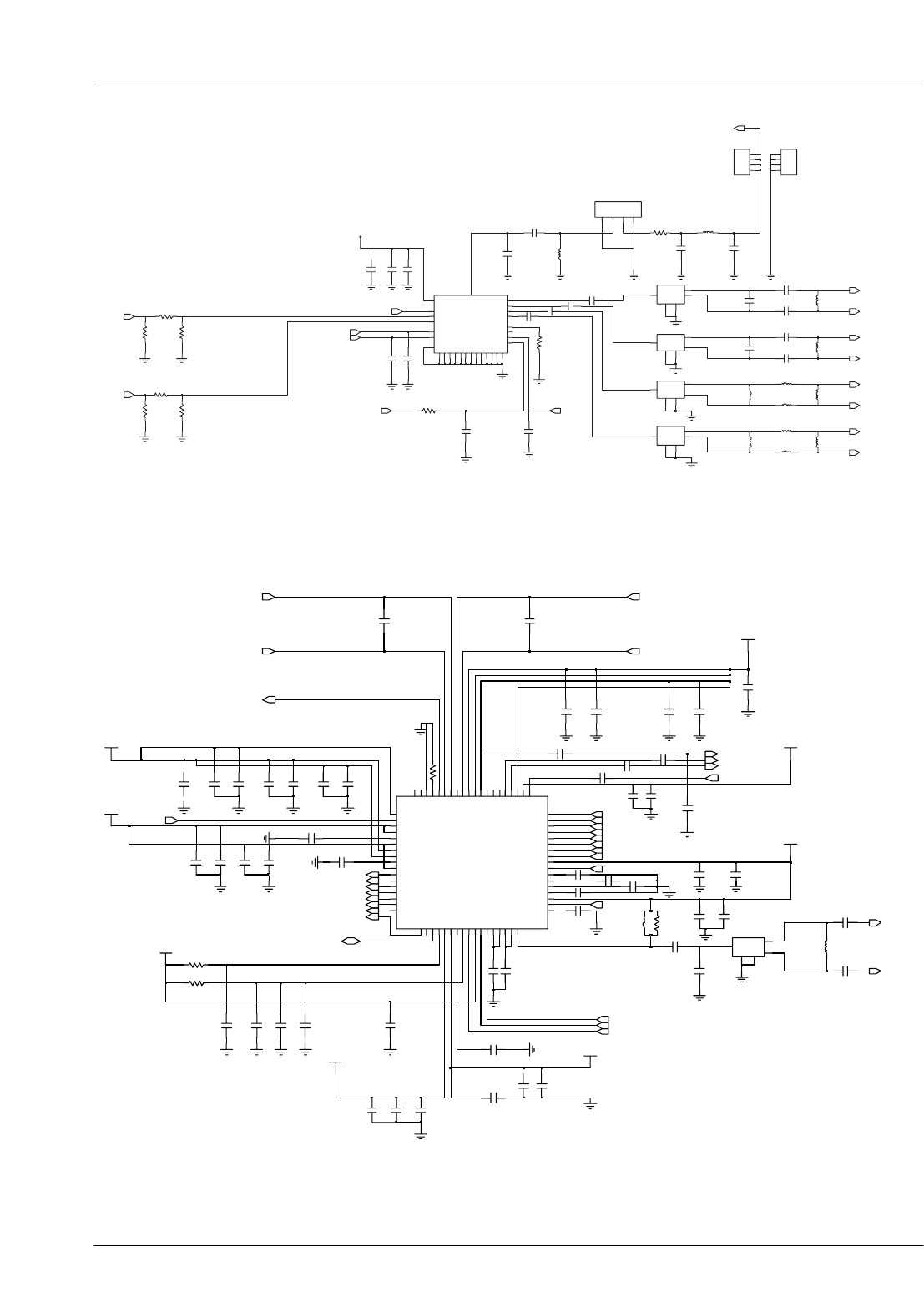
SAMSUNG Proprietary-Contents may change without notice
Flow Chart of Troubleshooting
10-33
This Document can not be used without Samsung’s authorization
22pFC147
25V
C164
22pF
25V
F
p
2
2
1
6
1
C
V
5
2
F
p
2
2
0
6
1
C
V
5
2
100PF
25V
C153
5.6
R112
VRFRX2_2.7V
10V
100NF
C140
25V
22pF
C125
C141
22pF
25V
VRFRX1_2.1V
VRFRX1_2.1V
C1113
22pF
25V
C123
6.3V
100nF 100nF
C126
6.3V 6.3V
100nF
C129
C146
25V
22pF
C133
1NF
16V
C139
C132
25V 10V
100NF
25V
C148
100PF
22pF
0.068NF
C100
25V
C1114
22pF 25V
C106
100NF
10V
100PF
25V
C105
C173
10V
100NF
C116 100PF
25V
25V
22pF
R101
12K
C177
C127
25V
100PF
VRFRX1_2.1V
100PF
C128
25V
C152
25V
3.9PF
C115
25V
22pF
C144
33PFC117
33PF
25V
25V
VRFRX2_2.7V
4.7pF
C157
NC
C130
10V
100NF
C178
C190
0.0003nF
10V
100NF
C102
100NF
C154
10V
100NF
C149
10V
C134
10V
10nF
C162
4700NF
10V
R111
10V
5.6
10nH
4700NF
C163
L114
25V
3.9PF
C159
50V
1NF
C176
3
OUT
OUT 4
F104
FAR-F6KB-2G1400-B4GCHZ
G
2
G
5
1IN
G
U
L
S
_
D
N
G9
6
VDDA2
7
C
N0
7
C
N1
7
VDDA2
8
9VTUNE_GPS
2
A
D
D
V1
6
2
A
D
D
V2
6
N
I
_
X
T3
6
PI
_
X
T4
6
N
Q
_
X
T5
6
P
Q
_
X
T6
6
F
E
R
I
_
C
A
D7
6
S
A
I
B
R
_
X
T8
6
2
A
D
D
V4
5
1
T
U
O
_
F
R
_
B
L5
5
1
T
U
O
_
F
R
_
B
H6
5
2
T
U
O
_
F
R
_
B
L7
5
2
T
U
O
_
F
R
_
B
H8
5
3
T
U
O
_
F
R
_
B
H9
5
VDDA1
6
2
A
D
D
V0
6
DCS_INN 47
EGSM_INP 48
EGSM_INN 49
VTUNE1
5
GCELL_INP 50
51
GCELL_INN
2
5
PDET_IN
1
A
D
D
V3
5
39
VDDA1
4
WDRXHB1 40
WDRXLB 41
GPS_IN 42
VDDA2 43
GPCS_INP 44
45
GPCS_INN
DCS_INP 46
1
3
P
B
H
X
R
P
W
2
3
M
B
H
X
R
P
W
3
3
T
U
O
_
2
E
S
X
R
P
W
4
3
WPRXSE1_OUT
35
WPRXSE2 36
VDDA2 37
WPRXSE1 38
WDRXHB2
2
A
D
D
V
5
2
N
O
_
F
R
6
2
2
A
D
D
V
7
2
P
NI
_
X
M
_
B
W
8
2
M
NI
_
X
M
_
B
W
9
2
VDDA1
3
P
B
L
X
R
P
W
0
3
M
B
L
X
R
P
W
8
1NI
_
X
R
D
9
1C
|
N
TCXO
2
T
D
B
S
0
2
2
A
D
D
V
1
2
1
A
D
D
V
2
2
3
2M
D
D
V
2
E
N
U
T
V
4
2
10 VDDA1
PRX_QP
11
PRX_QN
12
PRX_IN
13
PRX_IP
14
DRX_QP
15
DRX_QN
16
DRX_IP
17
U100
RTR6285
VDDA2
1
L110
2.2nH
C166
100PF
25V
100NF
C108
25V
C172
10V
100PF
25V
100PF
VRFRX2_2.7V
C143
VMSMP_2.6V
C101
25V
0.068NF
6.3V
100nF
C165
22pF
25V
VRFRX1_2.1V
1K
C171
R110
6.3V
100nF
C124
10nFC167
100PF
C107
25V
10V
C142
10V
100NF
22pF C1112
25V
GSM850_RXP
GSM850_RXM
UMTS_RXP_2100
UMTS_RXM_2100
RTR6285_TCXO
SSBDT_RTR
UMTS_RXP_2100
UMTS_RXM_2100
WCDMA_IMT_RX
DAC_REF
RFOUT_GCELL_EGSM
RFOUT_DCS_PCS
RX_Q_P
RX_Q_N
RX_I_P
RX_I_N
RX1_I_P
RX1_I_N
RX1_Q_N
RX1_Q_P
TX_ON
RFOUT_IMT
TX_I_N
TX_I_PTX_Q_N
TX_Q_P
GSM_RXP
GSM_RXM
PCS_RXP
PCS_RXM
DCS_RXP
DCS_RXM
PWR_DET
RX_GPS
11
2
23
34
4
R106
ANT100
C110
L105
C112
C155
R102
G
5
G
1IN
3
OUT
OUT 4
F100
2
C121
C138
C114
1
3
OUT
OUT 4
F101
G
2
G
5
IN
L104
L101
C137
G
2
G
5
1IN
OUT 3
OUT 4
F103 L109
C156
R100
C118 L103
C109
44
ANT101
1
1
22
33
G
2 5
G
1IN
OUT 3
4
OUT
F102
C131
L111
V_DC
L107
RX2
6
7
RX1
8
T
N
A
D
N
G
9
C135
25
VAPC
VBATT
26
BS2
27
28 BS1
GND29
3
RSVD
4
RX4
RX3
5
8
1D
N
G
9
1
D
N
G
2
MODE
D
N
G
0
2
21 DCS|PCS_IN
D
N
G
2
2
23
GSM_IN
D
N
G
4
2
10
WCDMA1
1
1D
N
G
D
N
G
2
1
D
N
G
3
1
D
N
G
4
1
D
N
G
5
1
6
1
D
N
G
7
1
D
N
G
PAM100
_TXEN 1
RFS100
2A
3C
1G
4G
R104
C122
L108
L102
C103
C136
L106
L100
R105
R107
L112
C145
C111
R103
R108
C120
C119
C150
R109
C113
TRX_WCDMA2100
PCS_RXM
GSM_RXP
GSM_RXM
GSM850_RXM
GSM850_RXP
PAM_RAMP+
GSM_ANT_SEL2_N
GSM_ANT_SEL1_N
DCS_RXP
DCS_RXM
PCS_RXP
RFOUT_DCS_PCS
RFOUT_GCELL_EGSM
GSM_ANT_SEL0_N
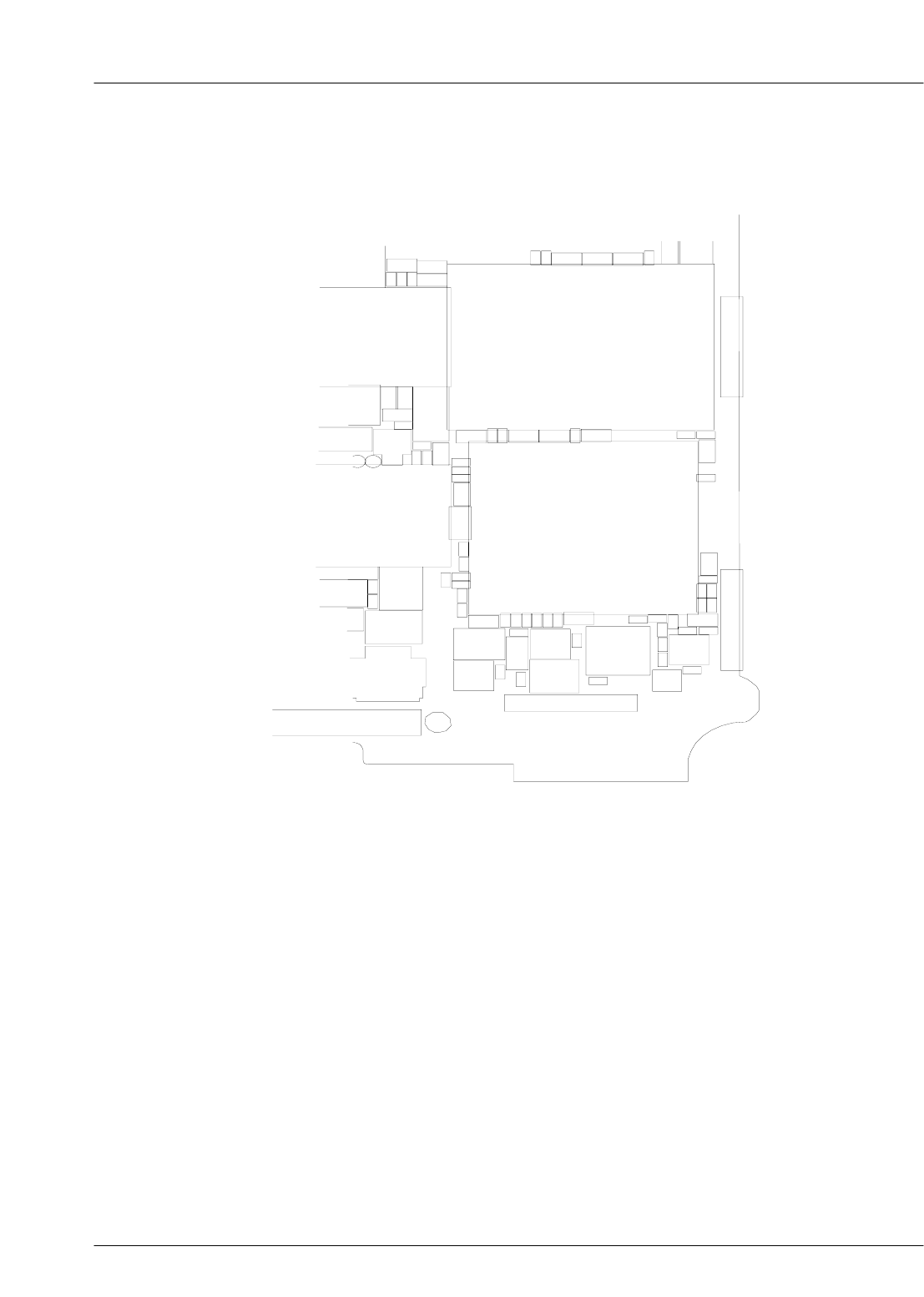
SAMSUNG Proprietary-Contents may change without notice
Flow Chart of Troubleshooting
10-34
This Document can not be used without Samsung’s authorization
C20 0
1
0
2
C
C202
3
0
2
C
4
0
2
C
5
0
2
C
C206C207
C20 8
9
0
2
C
C210
C21 1 C21 2
C21 3
C21 4
5
1
2
C
6
1
2
C
7
1
2
C
C218
9
1
2
C
0
2
2
C
1
2
2
C
2
2
2
C
3
2
2
C
4
2
2
C
C22 5C22 6
7
2
2
C
8
2
2
C
2
2
C
1
3
2
C
C23 2
3
3
2
C
5
3
2
C
C23 6
7
3
2
C
8
3
2
C
1
4
2
C
2
4
2
C
3
4
2
C
C244
5
4
2
C
6
4
2
C
6
0
3
C
8
0
3
C
C310
C31 4
C31 5
C31 6
C317
8
1
3
C
1
2
3
C
C32 2
C678
C679
2
8
6
C
CN201
D30 0
DF_AL EDF_CLE
1
0
3
L
MGND
0
0
3
C
S
O
R200
2
0
2
R
6
0
2
R
R20 7
8
0
2
R
9
0
2
R
R210
R211
R212
R213
4
1
2
R
5
1
2
R
6
1
2
R
7
1
2
R
R218
9
1
2
R
1
2
2
R
2
2
2
R
R30 2
3
0
3
R
R304
2
1
3
R
0
0
1
C
S
1
0
1
C
S
SC11 3
SLC50 1
0
0
3
A
T
0
0
6
R
T
U200
U201
2
0
2
U
3
0
2
U
5
0
2
U
U206
7
0
2
U
U20 8
U301
7
0
6
U
U61 0
0
0
2
P
C
U0
0
2
E
M
U
UME201
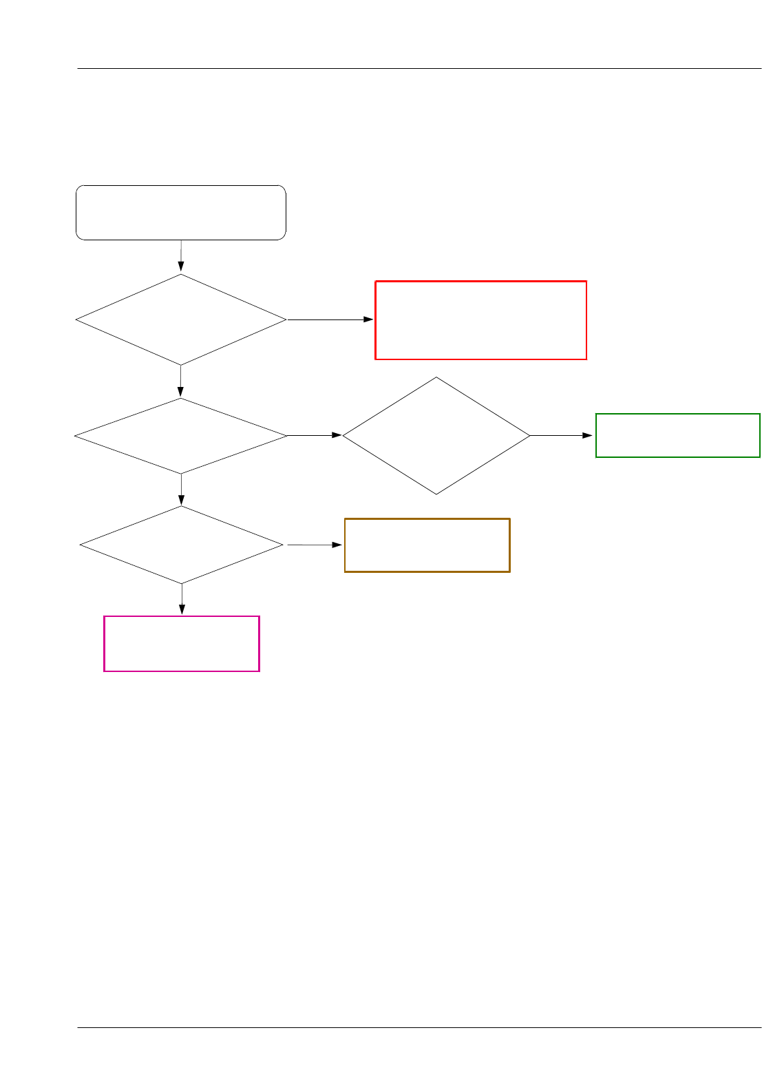
SAMSUNG Proprietary-Contents may change without notice
Flow Chart of Troubleshooting
10-35
This Document can not be used without Samsung’s authorization
10-12. DCS Receiver
RX ON
Sector PWR=50dBm
Resolder or change F102
L106, L107, L108
Check U100 &UCP200
PAM100 Pin8
>= -60dBm
Check PAM100
Truth Table
Pin 1:LOW
Pin 27 : HIGH
Pin 28 : LOW
No
Yes
Resolder RFS100, C103, R100, L100
,L101, C111
Resolder or change PAM100
No
PAM100 Pin 6
>= -70dBm
Yes
U100 Pin 46, 47
>= -75dBm
No
Yes
Yes
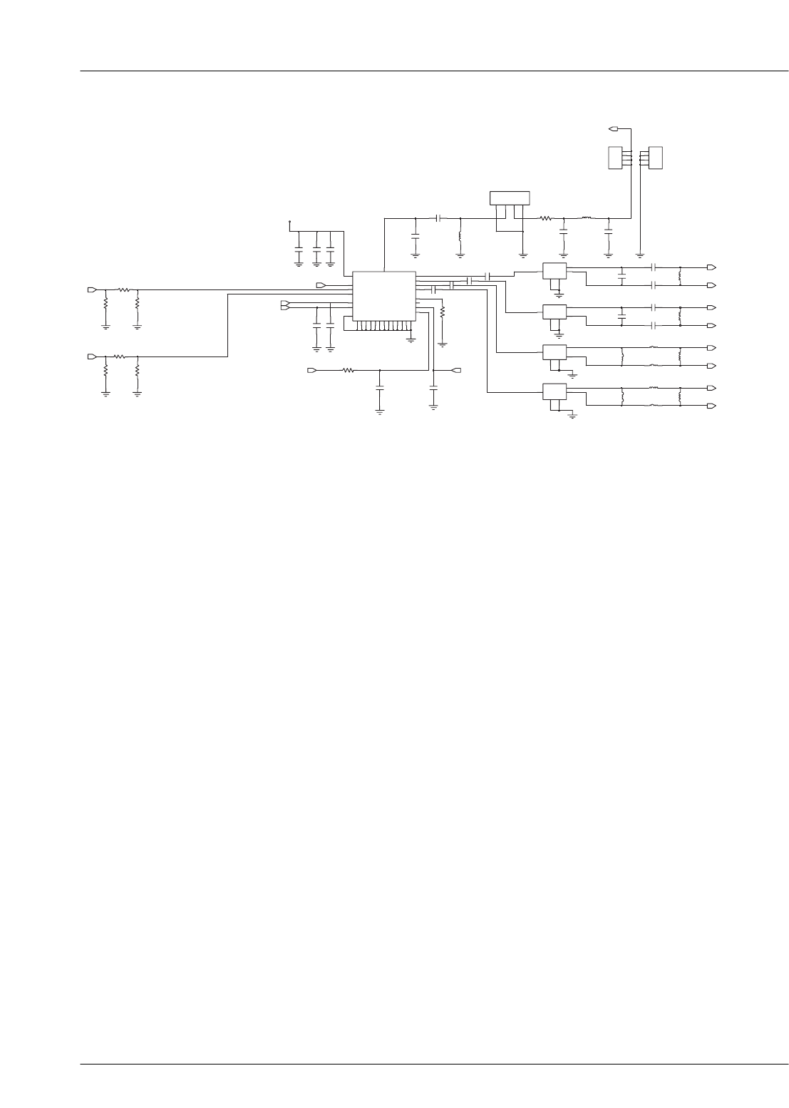
SAMSUNG Proprietary-Contents may change without notice
Flow Chart of Troubleshooting
10-36
This Document can not be used without Samsung’s authorization
11
2
23
34
4
R106
ANT100
C110
L105
C112
C155
R102
G
5
G
1IN
3
OUT
OUT 4
F100
2
C121
C138
C114
1
3
OUT
OUT 4
F101
G
2
G
5
IN
L104
L101
C137
G
2
G
5
1IN
OUT 3
OUT 4
F103 L109
C156
R100
C118 L103
C109
44
ANT101
1
1
22
33
G
2 5
G
1IN
OUT 3
4
OUT
F102
C131
L111
V_DC
L107
RX2
6
7
RX1
8
T
N
A
D
N
G
9
C135
25
VAPC
VBATT
26
BS2
27
28 BS1
GND29
3
RSVD
4
RX4
RX3
5
8
1D
N
G
9
1
D
N
G
2
MODE
D
N
G
0
2
21 DCS|PCS_IN
D
N
G
2
2
23
GSM_IN
D
N
G
4
2
10
WCDMA1
1
1D
N
G
D
N
G
2
1
D
N
G
3
1
D
N
G
4
1
D
N
G
5
1
6
1
D
N
G
7
1
D
N
G
PAM100
_TXEN 1
RFS100
2A
3C
1G
4G
R104
C122
L108
L102
C103
C136
L106
L100
R105
R107
L112
C145
C111
R103
R108
C120
C119
C150
R109
C113
T
TRX_WCDMA2100
PCS_RXM
GSM_RXP
GSM_RXM
GSM850_RXM
GSM850_RXP
PAM_RAMP+
GSM_ANT_SEL2_N
GSM_ANT_SEL1_N
DCS_RXP
DCS_RXM
PCS_RXP
RFOUT_DCS_PCS
RFOUT_GCELL_EGSM
GSM_ANT_SEL0_N
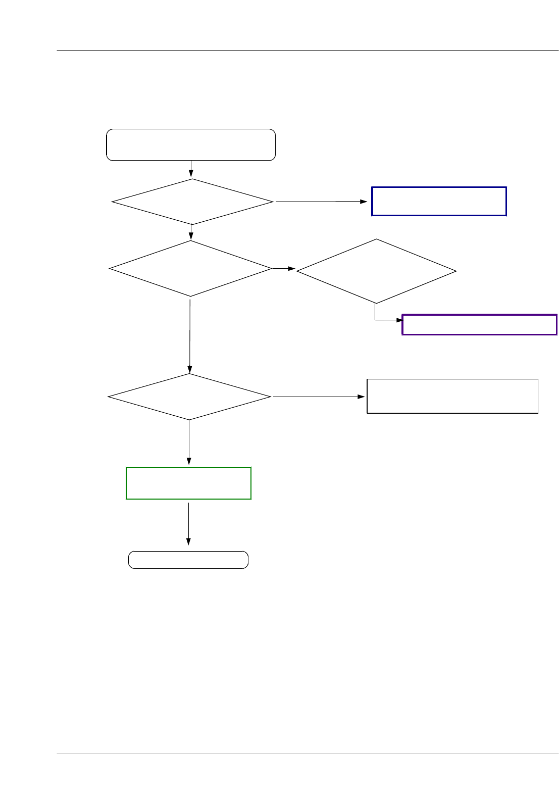
SAMSUNG Proprietary-Contents may change without notice
Flow Chart of Troubleshooting
10-37
This Document can not be used without Samsung’s authorization
10-13. DCS Transmitter
TX ON
(PCL 5level)
PAM100 Pin 21
>= 0dBm
PAM100 Pin 56
>= 0dBm
END
Resolder RFS100, C103, R100
,L100, L101, C111
Resolder or change PAM100
PAM100 Pin 8
>= 0dBm
Check F100 Truth Table
Pin 1:LOW
Pin 27 : HIGH
Pin 28 : HIGH
No
No
Yes
Yes
Yes
NO
YES
Resolder or change PAM100, R102
,R103 ,R104 ,R105
Check U100 &UCP200
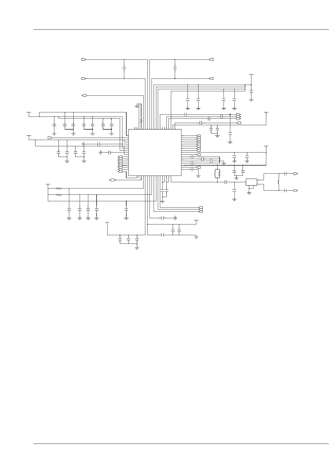
SAMSUNG Proprietary-Contents may change without notice
Flow Chart of Troubleshooting
10-38
This Document can not be used without Samsung’s authorization
C147
C164
1
6
1
C
0
6
1
C
C153
R112
VRFRX2_2.7V
C140
C125
C141
VRFRX1_2.1V
VRFRX1_2.1V
C1113
C123 C126 C129
C146
C133
C139
C132
C148
C100
C1114
C106C105
C173
C116
R101
C177
C127
VRFRX1_2.1V
C128
C152
C115
C144
C117
VRFRX2_2.7V
C157
C130
C178
C190
C102
C154
C149
C134
C162
R111
C163
L114
C159
C176
3
OUT
OUT 4
F104
G
2
G
5
1IN
G
U
L
S
_
D
N
G9
6
VDDA2
7
C
N0
7
C
N1
7
VDDA2
8
9VTUNE_GPS
2
A
D
D
V1
6
2
A
D
D
V2
6
N
I
_
X
T3
6
IP
_
X
T4
6
N
Q
_
X
T5
6
P
Q
_
X
T6
6
F
E
R
I
_
C
A
D7
6
S
A
I
B
R
_
X
T8
6
2
A
D
D
V4
5
1
T
U
O
_
F
R
_
B
L5
5
1
T
U
O
_
F
R
_
B
H6
5
2
T
U
O
_
F
R
_
B
L7
5
2
T
U
O
_
F
R
_
B
H8
5
3
T
U
O
_
F
R
_
B
H9
5
VDDA1
6
2
A
D
D
V0
6
DCS_INN 47
EGSM_INP 48
EGSM_INN 49
VTUNE1
5
GCELL_INP 50
51
GCELL_INN
2
5
PDET_IN
1
A
D
D
V3
5
39
VDDA1
4
WDRXHB1 40
WDRXLB 41
GPS_IN 42
VDDA2 43
GPCS_INP 44
45
GPCS_INN
DCS_INP 46
1
3
P
B
H
X
R
P
W
2
3
M
B
H
X
R
P
W
3
3
T
U
O
_
2
E
S
X
R
P
W
4
3
WPRXSE1_OUT
35
WPRXSE2 36
VDDA2 37
WPRXSE1 38
WDRXHB2
2
A
D
D
V
5
2
N
O
_
F
R
6
2
2
A
D
D
V
7
2
P
IN
_
X
M
_
B
W
8
2
M
IN
_
X
M
_
B
W
9
2
VDDA1
3
P
B
L
X
R
P
W
0
3
M
B
L
X
R
P
W
8
1IN
_
X
R
D
9
1C
|
N
TCXO
2
T
D
B
S
0
2
2
A
D
D
V
1
2
1
A
D
D
V
2
2
3
2M
D
D
V
2
E
N
U
T
V
4
2
10 VDDA1
PRX_QP
11
PRX_QN
12
PRX_IN
13
PRX_IP
14
DRX_QP
15
DRX_QN
16
DRX_IP
17
U100
VDDA2
1
L110
C166
C108
C172
VRFRX2_2.7V
C143
VMSMP_2.6V
C101
25V
0.068NF
C165
VRFRX1_2.1V
C171
R110
C124
C167
C107
C142
C1112
GSM850_RXP
GSM850_RXM
UMTS_RXP_2100
UMTS_RXM_2100
RTR6285_TCXO
SSBDT_RTR
UMTS_RXP_2100
UMTS_RXM_2100
WCDMA_IMT_RX
DAC_REF
RFOUT_GCELL_EGSM
RFOUT_DCS_PCS
RX_Q_P
RX_Q_N
RX_I_P
RX_I_N
RX1_I_P
RX1_I_N
RX1_Q_N
RX1_Q_P
TX_ON
RFOUT_IMT
TX_I_N
TX_I_PTX_Q_N
TX_Q_P
GSM_RXP
GSM_RXM
PCS_RXP
PCS_RXM
DCS_RXP
DCS_RXM
PWR_DET
RX_GPS
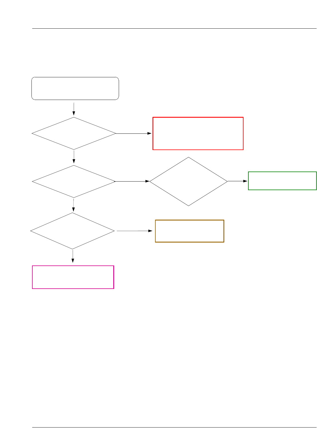
SAMSUNG Proprietary-Contents may change without notice
Flow Chart of Troubleshooting
10-39
This Document can not be used without Samsung’s authorization
10-14. PCS Receiver
RX ON
Sector PWR=50dBm
Resolder or change
F103, L109, L111, L112
Check U100 &UCP200
PAM100 Pin 8
>= -60dBm
Check PAM100
Truth Table
Pin 1:HIGH
Pin 27 : LOW
Pin 28 : LOW
No
Yes
Resolder RFS100, C103, R100
,L100, L101, C111
Resolder or change PAM100
No
PAM100 Pin 7
>= -70dBm
Yes
U100 Pin 44, 45
>= -75dBm
No
Yes
Yes
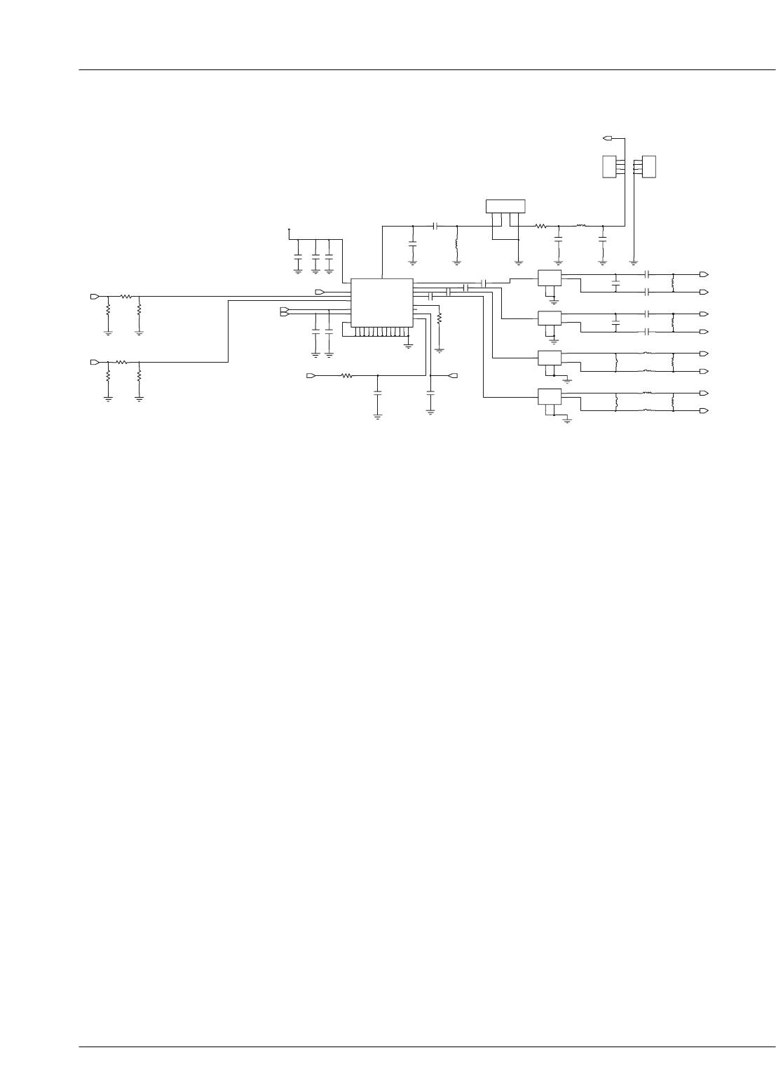
SAMSUNG Proprietary-Contents may change without notice
Flow Chart of Troubleshooting
10-40
This Document can not be used without Samsung’s authorization
11
2
23
34
4
R106
ANT100
C110
L105
C112
C155
R102
G
5
G
1IN
3
OUT
OUT 4
F100
2
C121
C138
C114
1
3
OUT
OUT 4
F101
G
2
G
5
IN
L104
L101
C137
G
2
G
5
1IN
OUT 3
OUT 4
F103 L109
C156
R100
C118 L103
C109
44
ANT101
1
1
22
33
G
2 5
G
1IN
OUT 3
4
OUT
F102
C131
L111
V_DC
L107
RX2
6
7
RX1
8
T
N
A
D
N
G
9
C135
25
VAPC
VBATT
26
BS2
27
28 BS1
GND29
3
RSVD
4
RX4
RX3
5
8
1D
N
G
9
1
D
N
G
2
MODE
D
N
G
0
2
21 DCS|PCS_IN
D
N
G
2
2
23
GSM_IN
D
N
G
4
2
10
WCDMA1
1
1D
N
G
D
N
G
2
1
D
N
G
3
1
D
N
G
4
1
D
N
G
5
1
6
1
D
N
G
7
1
D
N
G
PAM100
_TXEN 1
RFS100
2A
3C
1G
4G
R104
C122
L108
L102
C103
C136
L106
L100
R105
R107
L112
C145
C111
R103
R108
C120
C119
C150
R109
C113
T
TRX_WCDMA2100
PCS_RXM
GSM_RXP
GSM_RXM
GSM850_RXM
GSM850_RXP
PAM_RAMP+
GSM_ANT_SEL2_N
GSM_ANT_SEL1_N
DCS_RXP
DCS_RXM
PCS_RXP
RFOUT_DCS_PCS
RFOUT_GCELL_EGSM
GSM_ANT_SEL0_N
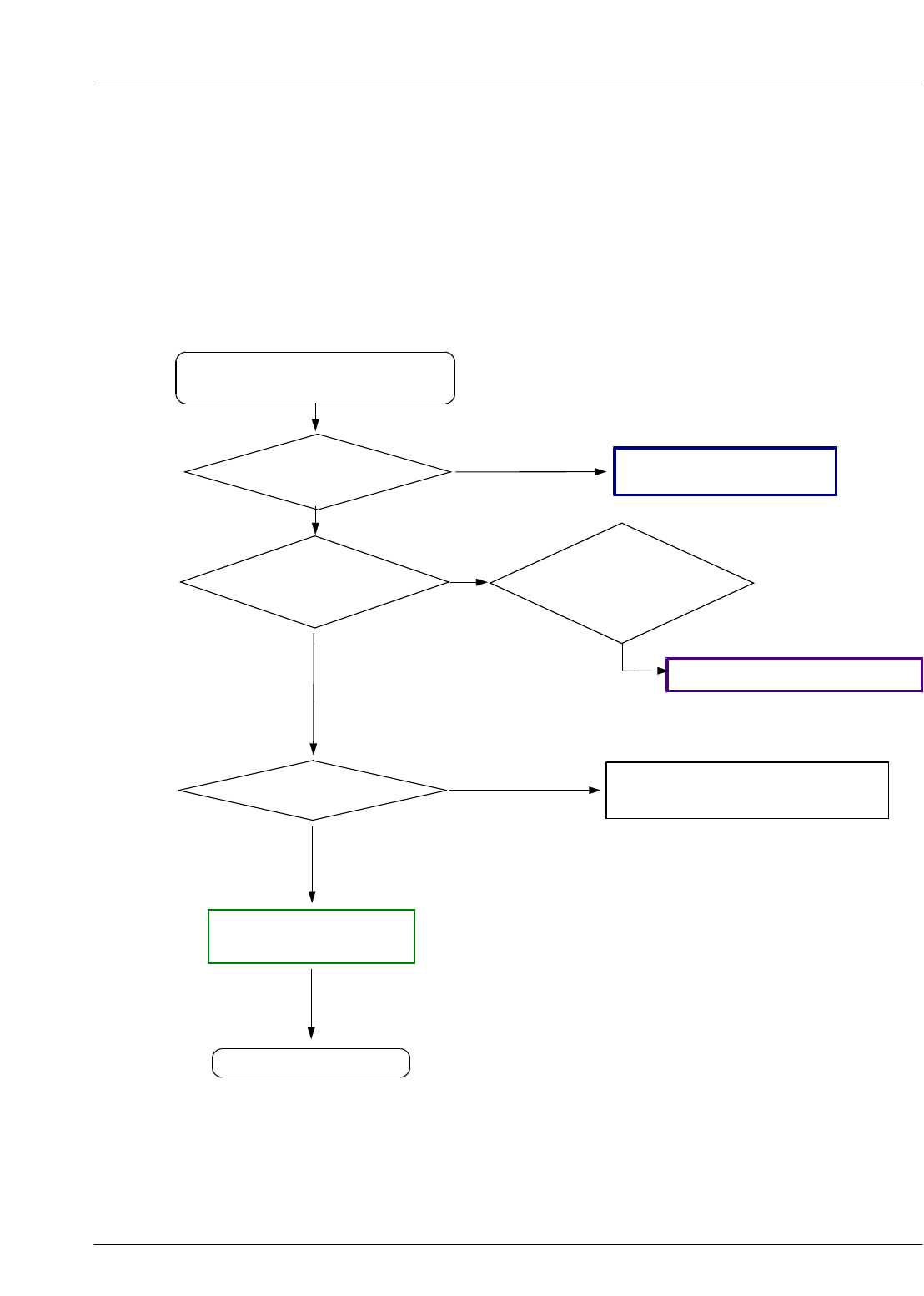
SAMSUNG Proprietary-Contents may change without notice
Flow Chart of Troubleshooting
10-41
This Document can not be used without Samsung’s authorization
10-15. PCS Transmitter
TX ON
(PCL 5level)
PAM100 Pin 21
>= 0dBm
PAM100 Pin 16
>= 0dBm
END
Resolder RFS100, C103, R100
,L100, L101, C111
Resolder or change PAM100
PAM100 Pin 8
>= 0dBm
Check PAM100
Truth Table
Pin 1:LOW
Pin 27 : HIGH
Pin 28 : HIGH
No
No
Yes
Yes
Yes
NO
YES
Resolder or change R102, R103
,R104 ,R105
Check U100 &UCP200
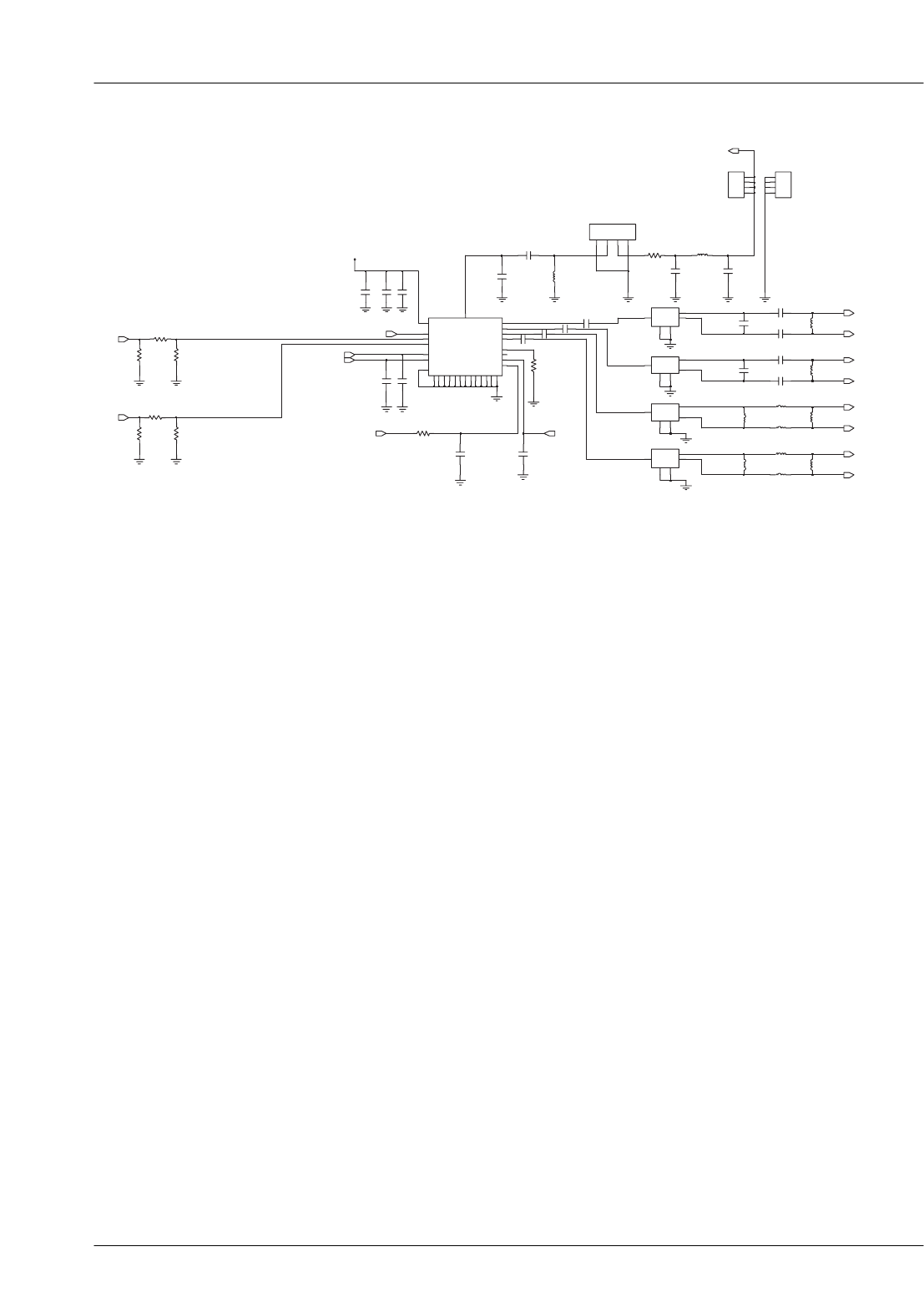
SAMSUNG Proprietary-Contents may change without notice
Flow Chart of Troubleshooting
10-42
This Document can not be used without Samsung’s authorization
11
2
23
34
4
R106
ANT100
C110
L105
C112
C155
R102
G
5
G
1IN
3
OUT
OUT 4
F100
2
C121
C138
C114
1
3
OUT
OUT 4
F101
G
2
G
5
IN
L104
L101
C137
G
2
G
5
1IN
OUT 3
OUT 4
F103 L109
C156
R100
C118 L103
C109
44
ANT101
1
1
22
33
G
2 5
G
1IN
OUT 3
4
OUT
F102
C131
L111
V_DC
L107
RX2
6
7
RX1
8
T
N
A
D
N
G
9
C135
25
VAPC
VBATT
26
BS2
27
28 BS1
GND29
3
RSVD
4
RX4
RX3
5
8
1D
N
G
9
1
D
N
G
2
MODE
D
N
G
0
2
21 DCS|PCS_IN
D
N
G
2
2
23
GSM_IN
D
N
G
4
2
10
WCDMA1
1
1D
N
G
D
N
G
2
1
D
N
G
3
1
D
N
G
4
1
D
N
G
5
1
6
1
D
N
G
7
1
D
N
G
PAM100
_TXEN 1
RFS100
2A
3C
1G
4G
R104
C122
L108
L102
C103
C136
L106
L100
R105
R107
L112
C145
C111
R103
R108
C120
C119
C150
R109
C113
NT
TRX_WCDMA2100
PCS_RXM
GSM_RXP
GSM_RXM
GSM850_RXM
GSM850_RXP
PAM_RAMP+
GSM_ANT_SEL2_N
GSM_ANT_SEL1_N
DCS_RXP
DCS_RXM
PCS_RXP
RFOUT_DCS_PCS
RFOUT_GCELL_EGSM
GSM_ANT_SEL0_N
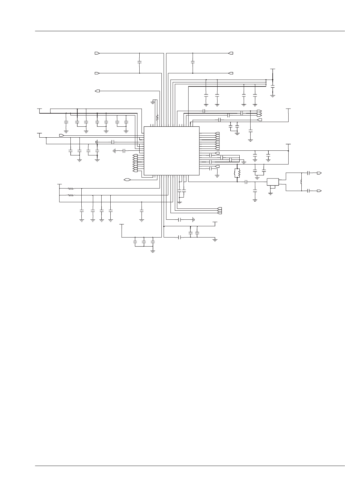
SAMSUNG Proprietary-Contents may change without notice
Flow Chart of Troubleshooting
10-43
This Document can not be used without Samsung’s authorization
C147
C164
1
6
1
C
0
6
1
C
C153
R112
VRFRX2_2.7V
C140
C125
C141
VRFRX1_2.1V
VRFRX1_2.1V
C1113
C123 C126 C129
C146
C133
C139
C132
C148
C100
C1114
C106C105
C173
C116
R101
C177
C127
VRFRX1_2.1V
C128
C152
C115
C144
C117
VRFRX2_2.7V
C157
C130
C178
C190
C102
C154
C149
C134
C162
R111
C163
L114
C159
C176
3
OUT
OUT 4
F104
G
2
G
5
1IN
G
U
L
S
_
D
N
G9
6
VDDA2
7
C
N0
7
C
N1
7
VDDA2
8
9VTUNE_GPS
2
A
D
D
V1
6
2
A
D
D
V2
6
N
I
_
X
T3
6
IP
_
X
T4
6
N
Q
_
X
T5
6
P
Q
_
X
T6
6
F
E
R
I
_
C
A
D7
6
S
A
I
B
R
_
X
T8
6
2
A
D
D
V4
5
1
T
U
O
_
F
R
_
B
L5
5
1
T
U
O
_
F
R
_
B
H6
5
2
T
U
O
_
F
R
_
B
L7
5
2
T
U
O
_
F
R
_
B
H8
5
3
T
U
O
_
F
R
_
B
H9
5
VDDA1
6
2
A
D
D
V0
6
DCS_INN 47
EGSM_INP 48
EGSM_INN 49
VTUNE1
5
GCELL_INP 50
51
GCELL_INN
2
5
PDET_IN
1
A
D
D
V3
5
39
VDDA1
4
WDRXHB1 40
WDRXLB 41
GPS_IN 42
VDDA2 43
GPCS_INP 44
45
GPCS_INN
DCS_INP 46
1
3
P
B
H
X
R
P
W
2
3
M
B
H
X
R
P
W
3
3
T
U
O
_
2
E
S
X
R
P
W
4
3
WPRXSE1_OUT
35
WPRXSE2 36
VDDA2 37
WPRXSE1 38
WDRXHB2
2
A
D
D
V
5
2
N
O
_
F
R
6
2
2
A
D
D
V
7
2
P
IN
_
X
M
_
B
W
8
2
M
IN
_
X
M
_
B
W
9
2
VDDA1
3
P
B
L
X
R
P
W
0
3
M
B
L
X
R
P
W
8
1IN
_
X
R
D
9
1C
|
N
TCXO
2
T
D
B
S
0
2
2
A
D
D
V
1
2
1
A
D
D
V
2
2
3
2M
D
D
V
2
E
N
U
T
V
4
2
10 VDDA1
PRX_QP
11
PRX_QN
12
PRX_IN
13
PRX_IP
14
DRX_QP
15
DRX_QN
16
DRX_IP
17
U100
VDDA2
1
L110
C166
C108
C172
VRFRX2_2.7V
C143
VMSMP_2.6V
C101
25V
0.068NF
C165
VRFRX1_2.1V
C171
R110
C124
C167
C107
C142
C1112
GSM850_RXP
GSM850_RXM
UMTS_RXP_2100
UMTS_RXM_2100
RTR6285_TCXO
SSBDT_RTR
UMTS_RXP_2100
UMTS_RXM_2100
WCDMA_IMT_RX
DAC_REF
RFOUT_GCELL_EGSM
RFOUT_DCS_PCS
RX_Q_P
RX_Q_N
RX_I_P
RX_I_N
RX1_I_P
RX1_I_N
RX1_Q_N
RX1_Q_P
TX_ON
RFOUT_IMT
TX_I_N
TX_I_PTX_Q_N
TX_Q_P
GSM_RXP
GSM_RXM
PCS_RXP
PCS_RXM
DCS_RXP
DCS_RXM
PWR_DET
RX_GPS
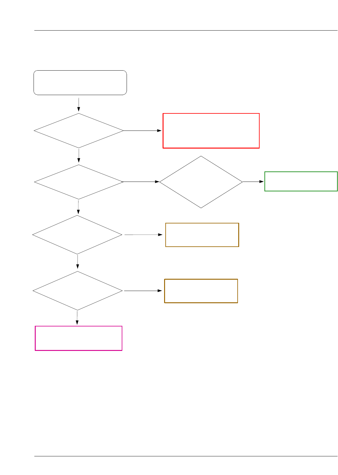
SAMSUNG Proprietary-Contents may change without notice
Flow Chart of Troubleshooting
10-44
This Document can not be used without Samsung’s authorization
10-16. WCDMA Receiver
RX ON
Sector PWR =-50
dBm
Resolder L115, C174, C179
Change U100 &F104 &UCP200
PAM100 Pin 8
>= -60dBm
Check PAM100
Truth Table
Pin 1:LOW
Pin 27 : LOW
Pin 28 : HIGH
No
Yes
Resolder RFS100, C103, R100
,L100, L101, C111
Resolder or change PAM100
No
PAM100 Pin 10
>= -70dBm
Yes
DUP100 Pin 2
>= -75dBm
No
Yes
Yes
DUP100 Pin 2
>= -75dBm
Yes
Resolder or change L126,
C189, DUP100
No
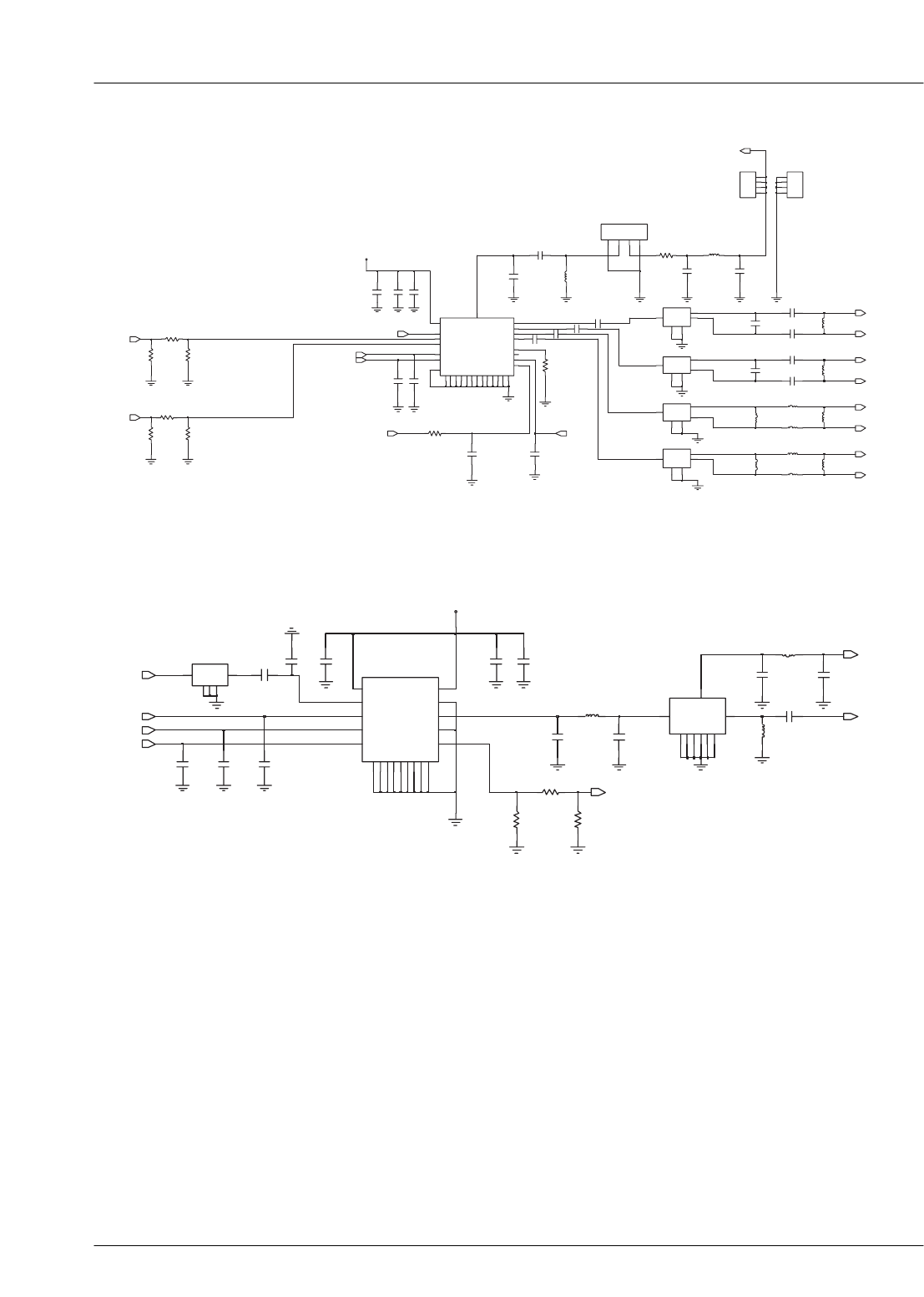
SAMSUNG Proprietary-Contents may change without notice
Flow Chart of Troubleshooting
10-45
This Document can not be used without Samsung’s authorization
C180
C179
C184
C151
C168
C170
V_DC
C169
C1111
L115
C181
C183
R116
R118
L116
F105
2
G G
3 5
G
IN
1
OUT
4
R117
RFIN
8
RFOUT
VCC1 011 VCC2
4VMODE0
VMODE1
3
12
D
N
G
D
N
G
13
D
N
G
1415
D
N
G
16
D
N
GD
N
G
17 19
C
N
2
6
CPLEN
5
GND 9
D
N
G
18
GND 7
D
N
G
11
PAM101
C1110
C174
C182
6
G
8 9
G
7
RX
5TX
DUP100
2
ANT
1
G
G
3 4
G
G
L126
PAM_R1
PWR_DET
WCDMA_IMT_RX
TRX_WCDMA2100
PAM_R0
RFOUT_IMT
PAM_ON0
11
2
23
34
4
R106
ANT100
C110
L105
C112
C155
R102
G
5
G
1IN
3
OUT
OUT 4
F100
2
C121
C138
C114
1
3
OUT
OUT 4
F101
G
2
G
5
IN
L104
L101
C137
G
2
G
5
1IN
OUT 3
OUT 4
F103 L109
C156
R100
C118 L103
C109
44
ANT101
1
1
22
33
G
2 5
G
1IN
OUT 3
4
OUT
F102
C131
L111
V_DC
L107
RX2
6
7
RX1
8
T
N
A
D
N
G
9
C135
25
VAPC
VBATT
26
BS2
27
28 BS1
GND29
3
RSVD
4
RX4
RX3
5
8
1D
N
G
9
1
D
N
G
2
MODE
D
N
G
0
2
21 DCS|PCS_IN
D
N
G
2
2
23
GSM_IN
D
N
G
4
2
10
WCDMA1
1
1D
N
G
D
N
G
2
1
D
N
G
3
1
D
N
G
4
1
D
N
G
5
1
6
1
D
N
G
7
1
D
N
G
PAM100
_TXEN 1
RFS100
2A
3C
1G
4G
R104
C122
L108
L102
C103
C136
L106
L100
R105
R107
L112
C145
C111
R103
R108
C120
C119
C150
R109
C113
NT
TRX_WCDMA2100
PCS_RXM
GSM_RXP
GSM_RXM
GSM850_RXM
GSM850_RXP
PAM_RAMP+
GSM_ANT_SEL2_N
GSM_ANT_SEL1_N
DCS_RXP
DCS_RXM
PCS_RXP
RFOUT_DCS_PCS
RFOUT_GCELL_EGSM
GSM_ANT_SEL0_N
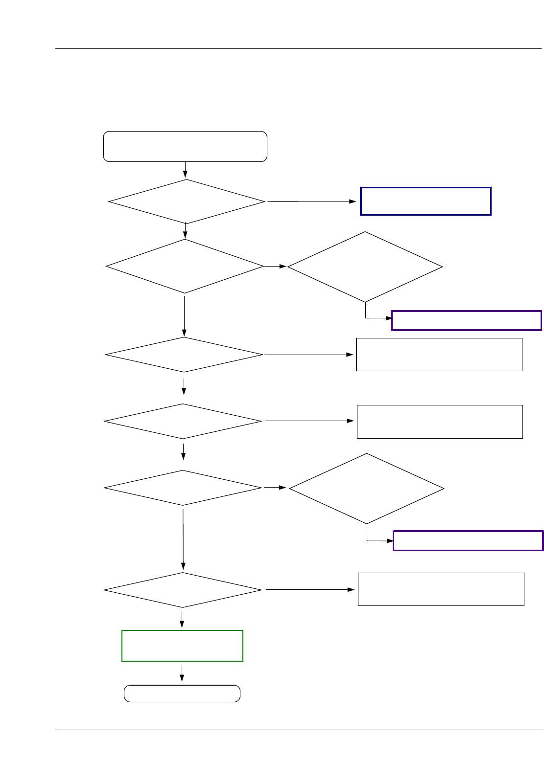
SAMSUNG Proprietary-Contents may change without notice
Flow Chart of Troubleshooting
10-46
This Document can not be used without Samsung’s authorization
10-17. WCDMA Transmitter
TX ON
(UE Target Power 24 dBm)
PAM100 Pin 10
>= 15dBm
DUP100 Pin 2
>= 15dBm
END
Resolder RFS100, C103, R100
,L100, L101, C111
Resolder or change PAM100
PAM100 Pin 8
>= 15dBm
Check PAM100
Truth Table
Pin 1:LOW
Pin 27 : LOW
Pin 28 : HIGH
No
No
Yes
Yes
Yes
NO
YES
Resolder L115, C174, C179
Check U100
Resolder or change DUP1—, L116, C111
PAM101 Pin 8
>= 15dBm
PAM101 Pin 2
>= 15dBm
U100 Pin 59
>= 15dBm
Yes
Check PAM100
Truth Table
Pin 3:LOW
Pin 4:LOW
Pin 5:HIGH
Yes
Resolder or change PAM101
YES
Resolder or change F105, C181, C112
Yes
NO
NO
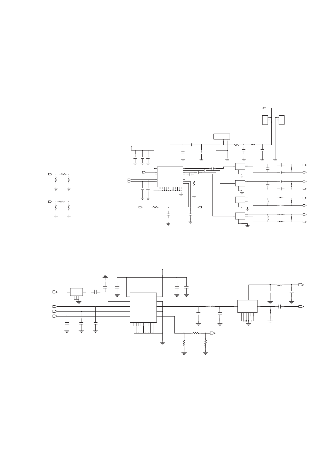
SAMSUNG Proprietary-Contents may change without notice
Flow Chart of Troubleshooting
10-47
This Document can not be used without Samsung’s authorization
C180
C179
C184
C151
C168
C170
V_DC
C169
C1111
L115
C181
C183
R116
R118
L116
F105
2
G G
3 5
G
IN
1
OUT
4
R117
RFIN
8
RFOUT
VCC1 011 VCC2
4VMODE0
VMODE1
3
12
D
N
G
D
N
G
13
D
N
G
1415
D
N
G
16
D
N
GD
N
G
17 19
C
N
2
6
CPLEN
5
GND 9
D
N
G
18
GND 7
D
N
G
11
PAM101
C1110
C174
C182
6
G
8 9
G
7
RX
5TX
DUP100
2
ANT
1
G
G
3 4
G
G
L126
PAM_R1
PWR_DET
WCDMA_IMT_RX
TRX_WCDMA2100
PAM_R0
RFOUT_IMT
PAM_ON0
11
2
23
34
4
R106
ANT100
C110
L105
C112
C155
R102
G
5
G
1IN
3
OUT
OUT 4
F100
2
C121
C138
C114
1
3
OUT
OUT 4
F101
G
2
G
5
IN
L104
L101
C137
G
2
G
5
1IN
OUT 3
OUT 4
F103 L109
C156
R100
C118 L103
C109
44
ANT101
1
1
22
33
G
2 5
G
1IN
OUT 3
4
OUT
F102
C131
L111
V_DC
L107
RX2
6
7
RX1
8
T
N
A
D
N
G
9
C135
25
VAPC
VBATT
26
BS2
27
28 BS1
GND29
3
RSVD
4
RX4
RX3
5
8
1D
N
G
9
1
D
N
G
2
MODE
D
N
G
0
2
21 DCS|PCS_IN
D
N
G
2
2
23
GSM_IN
D
N
G
4
2
10
WCDMA1
1
1D
N
G
D
N
G
2
1
D
N
G
3
1
D
N
G
4
1
D
N
G
5
1
6
1
D
N
G
7
1
D
N
G
PAM100
_TXEN 1
RFS100
2A
3C
1G
4G
R104
C122
L108
L102
C103
C136
L106
L100
R105
R107
L112
C145
C111
R103
R108
C120
C119
C150
R109
C113
NT
TRX_WCDMA2100
PCS_RXM
GSM_RXP
GSM_RXM
GSM850_RXM
GSM850_RXP
PAM_RAMP+
GSM_ANT_SEL2_N
GSM_ANT_SEL1_N
DCS_RXP
DCS_RXM
PCS_RXP
RFOUT_DCS_PCS
RFOUT_GCELL_EGSM
GSM_ANT_SEL0_N
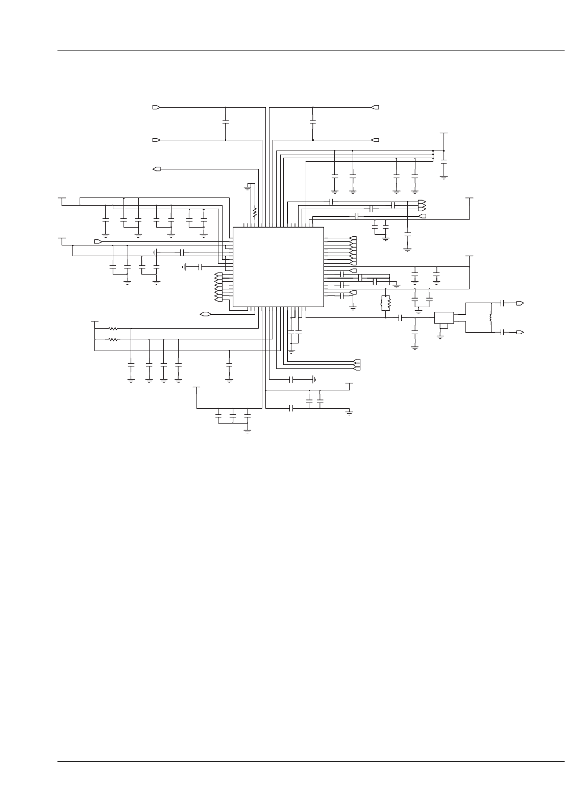
SAMSUNG Proprietary-Contents may change without notice
Flow Chart of Troubleshooting
10-48
This Document can not be used without Samsung’s authorization
C147
C164
1
6
1
C
0
6
1
C
C153
R112
VRFRX2_2.7V
C140
C125
C141
VRFRX1_2.1V
VRFRX1_2.1V
C1113
C123 C126 C129
C146
C133
C139
C132
C148
C100
C1114
C106C105
C173
C116
R101
C177
C127
VRFRX1_2.1V
C128
C152
C115
C144
C117
VRFRX2_2.7V
C157
C130
C178
C190
C102
C154
C149
C134
C162
R111
C163
L114
C159
C176
3
OUT
OUT 4
F104
G
2
G
5
1IN
G
U
L
S
_
D
N
G9
6
VDDA2
7
C
N0
7
C
N1
7
VDDA2
8
9VTUNE_GPS
2
A
D
D
V1
6
2
A
D
D
V2
6
N
I
_
X
T3
6
IP
_
X
T4
6
N
Q
_
X
T5
6
P
Q
_
X
T6
6
F
E
R
I
_
C
A
D7
6
S
A
I
B
R
_
X
T8
6
2
A
D
D
V4
5
1
T
U
O
_
F
R
_
B
L5
5
1
T
U
O
_
F
R
_
B
H6
5
2
T
U
O
_
F
R
_
B
L7
5
2
T
U
O
_
F
R
_
B
H8
5
3
T
U
O
_
F
R
_
B
H9
5
VDDA1
6
2
A
D
D
V0
6
DCS_INN 47
EGSM_INP 48
EGSM_INN 49
VTUNE1
5
GCELL_INP 50
51
GCELL_INN
2
5
PDET_IN
1
A
D
D
V3
5
39
VDDA1
4
WDRXHB1 40
WDRXLB 41
GPS_IN 42
VDDA2 43
GPCS_INP 44
45
GPCS_INN
DCS_INP 46
1
3
P
B
H
X
R
P
W
2
3
M
B
H
X
R
P
W
3
3
T
U
O
_
2
E
S
X
R
P
W
4
3
WPRXSE1_OUT
35
WPRXSE2 36
VDDA2 37
WPRXSE1 38
WDRXHB2
2
A
D
D
V
5
2
N
O
_
F
R
6
2
2
A
D
D
V
7
2
P
IN
_
X
M
_
B
W
8
2
M
IN
_
X
M
_
B
W
9
2
VDDA1
3
P
B
L
X
R
P
W
0
3
M
B
L
X
R
P
W
8
1IN
_
X
R
D
9
1C
|
N
TCXO
2
T
D
B
S
0
2
2
A
D
D
V
1
2
1
A
D
D
V
2
2
3
2M
D
D
V
2
E
N
U
T
V
4
2
10 VDDA1
PRX_QP
11
PRX_QN
12
PRX_IN
13
PRX_IP
14
DRX_QP
15
DRX_QN
16
DRX_IP
17
U100
VDDA2
1
L110
C166
C108
C172
VRFRX2_2.7V
C143
VMSMP_2.6V
C101
25V
0.068NF
C165
VRFRX1_2.1V
C171
R110
C124
C167
C107
C142
C1112
GSM850_RXP
GSM850_RXM
UMTS_RXP_2100
UMTS_RXM_2100
RTR6285_TCXO
SSBDT_RTR
UMTS_RXP_2100
UMTS_RXM_2100
WCDMA_IMT_RX
DAC_REF
RFOUT_GCELL_EGSM
RFOUT_DCS_PCS
RX_Q_P
RX_Q_N
RX_I_P
RX_I_N
RX1_I_P
RX1_I_N
RX1_Q_N
RX1_Q_P
TX_ON
RFOUT_IMT
TX_I_N
TX_I_PTX_Q_N
TX_Q_P
GSM_RXP
GSM_RXM
PCS_RXP
PCS_RXM
DCS_RXP
DCS_RXM
PWR_DET
RX_GPS

SAMSUNG Proprietary-Contents may change without notice
11. Reference data
11-1
This Document can not be used without Samsung’s authorization
11-1. Reference Abbreviate
AAC:Advanced Audio Coding.
AVC :Advanced Video Coding.
BER :Bit Error Rate
BPSK:Binary Phase Shift Keying
CA :Conditional Access
CDM :Code Division Multiplexing
C/I :Carrier to Interference
DMB :Digital Multimedia Broadcasting
EN :European Standard
ES :Elementary Stream
ETSI:European Telecommunications Standards Institute
MPEG:Moving Picture Experts Group
PN :Pseudo-random Noise
PS :Pilot Symbol
QPSK:Quadrature Phase Shift Keying
RS :Reed-Solomon
SI :Service Information
TDM :Time Division Multiplexing
TS :Transport Stream

www.s-manuals.com
-
Drivers
3
-
Repair manuals
1
-
User manuals
4

Samsung SGH-I900 service manual
(717 pages)
-
Type:
ZIP -
Size:
50.49 MB
Preview
Samsung SGH-I900 (Phones) service manuals in PDF format will help to find failures and errors and repair Samsung SGH-I900 and restore the device’s functionality.
|
Читать документ в PDF формате |
4.29 Мб |
Чтобы ваш телефон Samsung I900 WiTu 8Gb проработал долго и исправно рекомендуется почитать инструкцию по его эксплуатации.
Кажущиеся очевидными и простыми вещи зачастую оказываются более сложными и требуют внимательного изучения.
Руководство пользователя представлено на русском языке.
Выбрать инструкцию для другого телефона