Resources
| Knowledge Center | |
| ADS Support Home | |
| Documentation | |
| Downloads | |
| Licensing | |
| User Community | |
| Videos & eLearning |
Product Information
 |
Keysight EDA Home |
 |
ADS Products |
Current Release
The most up-to-date and complete documentation for the current release.
|
|
ADS 2023 Update 2 online documentation |
Current Release News
- What’s New in ADS
- ADS 2023 Update 2 Release Notes — For more information about this release
Installation Instructions
- Quick Install and License Setup
- Unix and Linux Installation Guide
- Windows Installation Guide
- Uninstall Instructions
Documentation for Previous Releases
Previous supported releases include up to two main releases back from the current release.
Welcome to the ADS Product Documentation
Access to the full set of on-line documentation for ADS requires you to have supported status. Your current status is: Unsupported.
SeeUnsupported statustroubleshooting tips.
Supported Releases
- ADS 2023 Update 1.0
- ADS 2023
- ADS 2022 Update 2.0
- ADS 2022 Update 1.0
- ADS 2022
- ADS 2021 Update 2.0
- ADS 2021 Update 1.0
- ADS 2021
- ADS 2020 Update 2.0
- ADS 2020 Update 1.0
- ADS 2020
Unsupported Releases
Previous unsupported versions are more than two main releases back from the current release.
The Release Documentation contains references to Agilent Technologies. Agilent’s former Test and Measurement business has become Keysight Technologies. For more information, go to
www.keysight.com.
- ADS 2019 Update 1.0
- ADS 2019
- ADS 2017 Update 1.0
- ADS 2017
- ADS 2016.01
- ADS 2015.01
- ADS 2014.01
- ADS 2013.06
- ADS 2012.08
- ADS 2011.10
- ADS 2011.05
- ADS 2011.01
- ADS 2009 Update 1
More…
- ADS 2009
- ADS 2008 Update 2
- ADS 2008 Update 1
- ADS 2008
- ADS 2006 Update 3
- ADS 2006 Update 2
- ADS 2006 Update 1
- ADS 2006
- ADS 2005A
- ADS 2004A
- ADS 2003C
- ADS 2003A
- ADS 2002C
- ADS 2002
- ADS 2001
- ADS 1.5
Программное обеспечение ADS — это полезный инструмент для дизайнеров, инженеров и предприятий, позволяющий быстро проектировать и производить высококачественные компоненты и системы.
Это программное обеспечение упрощает проектирование и моделирование деталей, независимо от их сложности. Кроме того, его легко освоить и адаптировать благодаря интуитивно понятному интерфейсу.
ADS произвел революцию в мире проектирования схем и систем для электроники, автомобилестроения и других отраслей, которые быстро внедряют это уникальное решение с готовыми функциями и возможностями.
Итак, давайте подробнее обсудим программное обеспечение ADS и выясним, как оно может вам помочь.
Что такое АДС?
Усовершенствованная система проектирования (ADS) — ведущее программное обеспечение для проектирования электронных схем, моделирования и автоматизации, разработанное компанией PathWave Design, принадлежащей Keysight Technologies.
Программное обеспечение ADS предлагает интегрированную среду для проектирования радиочастотных электронных систем, таких как беспроводные сети, мобильные телефоны, спутниковая связь, пейджеры, высокоскоростные каналы передачи данных и радиолокационные системы. Его первоначальный выпуск появился в 1985 году под названием Microwave Design System (MDS). ADS был представлен в 2016 году с улучшением скорости, производительности и гибкости дизайна.
Разработчики могут использовать ADS на каждом этапе процесса проектирования, от создания схемы, проверки правил проектирования и компоновки до моделирования электромагнитного поля и моделирования цепей во временной и частотной областях. Таким образом, разработчики могут легко охарактеризовать ВЧ-проекты и оптимизировать их без изменения каких-либо инструментов или систем.
Особенности рекламы
Некоторые из особенностей ADS заключаются в следующем:
- Шаблоны дизайна: ADS предоставляет вам интегрированную поддержку дизайна с помощью полезных шаблонов, которые вы можете использовать, чтобы быстро приступить к работе, не тратя много времени на каждый элемент дизайна при его создании с нуля.
- Библиотеки компонентов: вы получите обширную библиотеку компонентов, в которой вы сможете найти необходимую деталь для добавления в свой дизайн. Это также сэкономит много вашего времени. Все, что вам нужно сделать, это просмотреть различные компоненты и выбрать те, которые необходимы для вашего дизайна.
- Автоматическая синхронизация: ADS позволяет автоматически синхронизировать макет, чтобы визуализировать фактический макет при разработке схемы.
- Гибкость. Вы можете добиться большего успеха при проектировании, используя полный рабочий стол. Кроме того, включите ведущие промышленные и литейные разработки, чтобы сделать ваши проекты в соответствии с действующими стандартами. Вы также можете смоделировать нелинейный дизайн с помощью X-параметров. Если вам интересно, X-parameters является зарегистрированным товарным знаком Keysight в США, Японии, ЕС и других частях земного шара. X-параметры содержат уравнения и формат, помогающие при проектировании.
- Оптимизация дисплея: вы можете оптимизировать данные и дисплей кабины, чтобы получить то, о чем вы мечтали. Это также поможет вам увеличить производительность, поскольку вы можете визуализировать проекты и легко изменять их для создания высококачественных проектов без большого количества итераций.
- Интеграция: Вы можете интегрировать программное обеспечение ADS с электромагнитными симуляторами PathWave. Таким образом, вы можете получить четкое представление о своем дизайне с обзором на 360 градусов, а также определить, работает ли он в соответствии с ожиданиями. В результате вы можете найти области для улучшения и сделать свои проекты более эффективными.
- Управление: Программное обеспечение ADS будет содержать все данные, относящиеся к вашему проекту, компонентам и полной системе, которую вы хотите создать. Это также облегчит вам управление рабочим пространством для ускорения производства. Вы даже можете поделиться своим рабочим пространством и управлять им между своими командами.
Преимущества рекламы
Вот некоторые из преимуществ использования программного обеспечения ADS:
Обеспечивает уверенность в дизайне
Благодаря точным данным от ADS ваши команды могут визуализировать и определить, соответствуют ли их проекты требуемым спецификациям. Аналитика и визуализация данных программного обеспечения ADS включают в себя диаграммы, диаграммы и графики, которые помогут вам четко просматривать и анализировать данные, а также делать выводы и вносить изменения. А когда вы знаете недостатки своего дизайна, вы можете легко их исправить, что повысит вашу уверенность в дизайне.
Более быстрое производство

Ускорьте проектирование и быстро переходите к производству с помощью полезных шаблонов, мастеров и руководств по проектированию. Весь процесс проектирования будет включать в себя схемы, схемы, компоновку, электротермическое, электромагнитное моделирование и т. д.
Даже если ваша команда плохо знакома с программным обеспечением, им не составит труда адаптироваться к этому программному обеспечению. Они могут легко проектировать и улучшать каждый компонент и быстрее запускать его в производство. В результате время вашего выхода на рынок увеличивается.
Преодолейте проблемы высокоскоростного проектирования
Когда скорость и частота увеличиваются, мощность и целостность сигнала становятся более важными для печатных плат (PCB), поэтому, если в линии передачи возникают потери, это может привести к сбоям в работе электронных устройств.
Таким образом, моделирование межсоединений, дорожек и переходных отверстий имеет решающее значение для точного моделирования печатной платы. Для этого компания Keysight помогает повысить производительность высокоскоростных каналов связи в ваших печатных платах с помощью электромагнитных симуляторов и конструкций интегральных схем, адаптированных для анализа целостности сигналов и питания.
В результате вы получаете безупречный дизайн каждого компонента вашей системы и производите их, не задумываясь.
Повышает надежность конструкции
Надежность и эффективность — две основные вещи, которые необходимо учитывать при проектировании и производстве компонентов и машин.
Такие системы, как солнечные инверторы, электромобили и источники питания, нуждаются в эффективных конструкциях. Следовательно, компании ищут способы повышения эффективности и надежности силовых устройств еще на стадии проектирования. В этом вам могут помочь такие материалы, как нитрид галлия, карбид кремния и т. д. С помощью Keysight ADS вы можете моделировать импульсные источники питания и современные материалы, чтобы оптимизировать свои проекты и добиться максимальной эффективности.
Приложения для рекламы
Ниже обсуждаются области, в которых вы можете использовать программное обеспечение ADS.
Моделирование схемы
ADS 2016 — это мощное программное обеспечение, которое может усовершенствовать Harmonic Balance Engine и повысить точность, сходимость и скорость симуляторов цепей. Он также предлагает улучшенные аннотации DC, которые помогают ускорить производство даже сложных проектов.
Кроме того, поддержка Linux и Windows для электротермического моделирования повышает доступность этой системы практически для каждого проектировщика. Вы также можете выполнять моделирование на нескольких облачных серверах и использовать повышенную скорость и масштабируемость.
Кремний RFIC
ADS от Keysight помогает сократить количество отказов оборудования и связанные с ними расходы за счет интеллектуальной интеграции модулей, соединяющих системы проектирования схем, такие как радиочастотные интегральные схемы (RFIC), многослойные конструкции, антенны и монолитные микроволновые интегральные схемы (MMIC), корпуса на уровне пластин и печатные платы в плотные Трехмерные структуры.
ADS также помогает вам моделировать EVM для оптимизации и настройки, чтобы помочь вам проверить стандарты беспроводной связи на уровне отрасли, такие как автомобильные радары, 5G, WiFi и т. д. Благодаря всестороннему и тщательному анализу стабильности усилителя ADS заменяет традиционные методы, чтобы обеспечить повышенную стабильность усилителя в ненапряженных условиях. линейные и линейные условия.
Проверка макета
Новые возможности и усовершенствования, представленные в программном обеспечении ADS, делают макеты более быстрыми, надежными и интуитивно понятными. Были внесены улучшения с точки зрения управления и проверки производственной сетки, заземления цепей, средства просмотра 3D, подключения и выделения, сопоставления топологии с именами схемных цепей и импорта файла .brd для ЭМ-моделирования.
Он предлагает настоящие дуги для точного рисования или редактирования спиралей и изогнутых дорожек, автоматический экспорт/импорт GDSII, чтобы избежать ошибок пользователя, а также массовое редактирование различных структур, таких как формы, дорожки, контактные площадки, переходные отверстия и т. д., в одной сети. Вы даже можете проверить локальную плотность с помощью Design Rule Check (DRC).
Электротермический
ADS предлагает точное проектирование фильтров на ПАВ, а также моделирование графена. Вы можете использовать одну тепловую модель для разных импортированных проектов, чтобы улучшить совместимость потока.
Целостность питания
ADS обеспечивает моделирование электромагнитной совместимости, ориентированное на целостность сигнала, чтобы предлагать приложения высокой сложности и высокой точности для печатных плат, а также PIPro — симуляторы электромагнитной совместимости, ориентированные на целостность питания, для анализа сетей подачи электроэнергии.
Он также предлагает:
- Новый Sparse Direct Solver для ускорения моделирования на 40 % даже для сложных структур
- Кэширование сетки для сокращения времени моделирования
- Кэшированные графические интерфейсы для моделей компонентов, обеспечивающие простоту удаления или выбора
- Несколько VRM в одной симуляции DC IR Drop
Создание вашего первого дизайна с помощью программного обеспечения ADS может показаться сложной задачей. Но если вы знаете основы, вам станет легче, и тогда вы сможете продолжать практиковаться, чтобы достичь продвинутой стадии.
Давайте быстро перейдем к деталям того, как вы можете создать свой первый проект в ADS, а затем смоделировать и построить свои результаты.
Создать схемы
Начните с создания схемы нужной детали или компонента. Например, вы хотите создать фильтр нижних частот. Для этого вам сначала нужно добавить компонент, например резистор.
В ADS вы найдете библиотеку компонентов, которую вы можете использовать, чтобы найти готовый компонент и добавить его в свой проект. Это сэкономит вам много времени вместо того, чтобы создавать его с нуля. Существуют различные компоненты, которые упрощают и ускоряют проектирование, например, резисторы, конденсаторы, провода, соединения, элементы данных, источники измерений, контроллеры моделирования и т. д.
Кроме того, эти компоненты относятся к категории «Палитра». Еще проще переключать палитры с помощью раскрывающегося меню. Названия палитр говорят сами за себя, поэтому вы можете легко обнаружить и разместить их в своей среде проектирования. Например, если вы ищете резистор, конденсатор или катушку индуктивности, вы можете найти их в разделе «сосредоточенные компоненты». Если у вас возникли проблемы с поиском компонента, вы можете просмотреть его в алфавитном порядке в списке компонентов.
Разместите компонент
Найдя нужный компонент, например резистор, вы можете поместить его на свою схему. После выбора компонента он останется на курсоре. Следовательно, вы можете нажать клавишу ESC, чтобы остановить размещение того же компонента. После этого необходимо изменить параметры компонента, которые изначально определены по умолчанию. Вы можете сделать это, щелкнув значение по умолчанию и переписав значение в соответствии с вашими требованиями. Однако иногда вы не сможете увидеть значение по умолчанию. Для этого вы можете дважды щелкнуть этот компонент и просмотреть дополнительные свойства, которые нужно изменить.
Затем вы можете повторить те же шаги, когда добавляете другой компонент, например конденсатор или катушку индуктивности, из списка палитры. Также возможно изменить ориентацию компонента, повернув его на 90 градусов. Вы можете сделать это, найдя опцию на панели инструментов. Кроме того, вы можете изменить префикс единицы измерения.
Программное обеспечение Keysight ADS является гибким и простым в использовании благодаря функции перетаскивания. Если вы хотите сделать схему более четкой, вы можете перетаскивать ее, чтобы перемещать. Это не изменит ваши связи.
Синхронизируйте дизайн
Чтобы ваш схематический проект имел смысл, вы должны определить связи между вашими компонентами и то, как они размещены в вашем проекте. Это поможет вам синхронизировать ваш дизайн.
Например, вы можете подключить конденсатор к земле. Вы можете сделать это, выбрав «земля» на панели инструментов. Кроме того, вы можете вставить провод и подключить различные компоненты. Это поможет вам измерить выходное напряжение.
Моделирование
Для моделирования вам понадобится контроллер моделирования, чтобы определить цель моделирования. Вы можете найти различные типы контроллеров симуляции, такие как S-параметр, DC-AC, load pull, гармонический баланс и другие. Запустить симуляцию с программным обеспечением ADS также несложно.
Например, если вы хотите выполнить симуляцию как AC, перейдите на палитру симуляции AC и найдите контроллер симуляции AC.
Независимо от того, какой контроллер симуляции вы выберете, он будет иметь значок шестеренки. Итак, выберите контроллер симуляции по вашему выбору и измените настройки в соответствии с вашими требованиями к симуляции.
На этапе моделирования вам понадобятся различные элементы, такие как исходный компонент или метка. Выбрав исходный компонент, вы должны поместить его в среду моделирования. Как и прежде, измените значения выбранного вами компонента, установленного по умолчанию.
Однако вы можете выбрать «метку», если хотите легко рассчитать напряжение без использования пробника. Для использования метки, такой как метка провода, определите имя цепи, а затем добавьте его в то место, где вы хотите рассчитать напряжение.
Таким образом, вы можете создать полнофункциональную схему, готовую для моделирования. Итак, запустите симуляцию, используя горячую клавишу F7 на клавиатуре или панели инструментов. Теперь вы можете увидеть, как будет вести себя ваша схема при взаимодействии всех ее компонентов.
Заговор
После моделирования вы увидите страницу, на которой вы можете добавить свои уравнения и графики.
Вы можете выбрать различные типы графиков и диаграмм, например, диаграммы Смита, полярные графики и прямоугольные графики. Есть элемент, называемый переменной «vout» (обозначается как «v out»), измерение от размещенной метки.
Пример: Вы выбрали прямоугольный участок.
Теперь вы должны начать построение графика с определения осей x и y.
Здесь «vout» будет осью Y этого графика, а контроллер моделирования, такой как контроллер моделирования переменного тока, устанавливает частоту как ось X графика. Теперь вы можете отображать данные с помощью этого графика в ADS.
Вывод
Использование программного обеспечения ADS упрощает проектирование деталей и систем, будь то простые или сложные. Он не только предлагает уникальные функции и функции, но и прост в использовании для инженеров и дизайнеров.
Таким образом, если вы ищете хорошее программное решение для проектирования печатных плат, схем и многого другого, вы можете попробовать его. Он также предлагает бесплатную пробную версию, которую вы можете использовать, чтобы узнать, может ли она помочь вам решить ваши задачи проектирования и моделирования.
Description
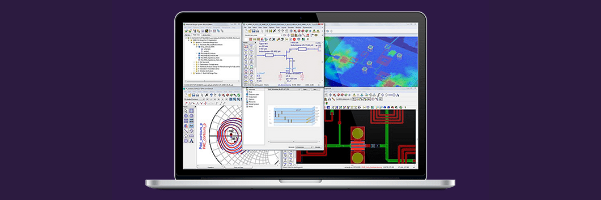
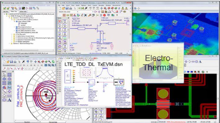
From Keysight Technologies’ Website: Pathwave Advanced Design System (ADS) offers integrated design guidance via templates to help you get started faster. Extensive component libraries make it easy to find the part you want. Automatic sync with layout allows you to visualize the physical layout while making schematic designs.
Version
- 2016_01
CIRCEaccount holdersRRAaccount holdersSCaccount holders
Platforms
CIRCEclusterRRAclusterSCcluster
Modules
Keysight ADS requires the following module file to run:
apps/ads/2016_01
- See Modules for more information.
Running Keysight ADS on CIRCE/SC
The Keysight ADS user guide is essential to understanding the application and making the most of it. The guide and this page should help you to get started with your simulations. Please refer to the Documentation section for a link to the guide.
- Note on CIRCE: Make sure to run your jobs from your $WORK directory!
- Note: Scripts are provided as examples only. Your SLURM executables, tools, and options may vary from the example below. For help on submitting jobs to the queue, see our SLURM User’s Guide.
Multiprocessor Graphical ADS
Establishing a GUI connection to CIRCE/SC
To use Keysight ADS, you will need to connect to CIRCE/SC with GUI redirection, either using:
- CIRCE/SC Desktop Environment
- SSH with X11 redirection
- If connecting from OSX or Linux via SSH, please ensure that you use one of the following commands to properly redirect X11:
-
[user@localhost ~]$ ssh -X circe.rc.usf.edu
or
-
[user@localhost ~]$ ssh -X sc.rc.usf.edu
-
- If connecting from OSX or Linux via SSH, please ensure that you use one of the following commands to properly redirect X11:
Once connected to CIRCE, you can open Jmol using the steps below:
[user@login0 ~]$ module load apps/ads/2016_01
[user@login0 ~]$ ads
Using Design Kits
To load currently installed design kits, click !DesignKit->List Design Kits, and enable the ones you would like to use.
To load you own design kits, follow the instructions below.
- Start ADS and install the design kit:
- From the ADS main window, click DesignKit->Install Design Kits
- Click Browse (next to Path) and locate the design kit library folder
- The rest of the information will fill in automatically
- Select USER LEVEL
- Click OK and the design kit will be installed.
- The new library design kit can now be run; the components can be selected from either the component pallet or component library.
Documentation
Home Page, User Guides, and Manuals
- Keysight ADS software page
- https://www.keysight.com/us/en/products/software/pathwave-design-software/pathwave-advanced-design-system.html
More Job Information
See the following for more detailed job submission information:
- SLURM User’s Guide
- Scheduling and Dispatch Policies
- Advanced Submit Techniques
Reporting Bugs
Report bugs with Keysight ADS to the IT Help Desk: rc-help@usf.edu
Getting Started with ADS
You’ve just downloaded ADS, and now you’d
like to get up and running in under 10 minutes.,Here’s how.,In this short video, you will learn how to
navigate through the ADS environment to create,a new workspace, build a new schematic, and
run a simulation.,Through an example, you will also learn how
to tune your design to optimize the performance.,You can use ADS with me along the way.,I’ll be using ADS 2016, but what you learn
in this video will generally apply to all,previous releases.,So let’s get started.,When you start ADS you will first see a getting
started screen.,There are many helpful resource links on this
page to explore if you are interested.,Let’s close it for now and Go ahead and
create a brand new workspace.,A workspace is how ADS organizes your design.,Click on the new workspace icon and follow
the on screen prompts.,Let’s give this workspace a name and set
up a few more parameters.,This is the point that you are going to decide:
Are you going to work on Analog RF domain,,DSP domain, or will you be doing something
that requires library parts from external,sources?,If you are doing IC design, you may need foundry
parts from foundries, and if you are doing,board design, you may need components such
as capacitors and inductors from component,vendors.,We are just getting started so I will accept the defaults.,This is an important choice if you are doing
a layout design; but for now, we are just,going to keep the default choice and click
Next.,Great!,Now the workspace is all set up and you have
a blank ADS workspace open.,Let’s start building our circuit.,You typically build in schematics.,So here is how to create a schematic window.,It can be helpful to use the wizard, but let’s ignore that for now.,Here is the schematic window in the middle
and library palette on the left.,From the palatte, you can place components
on your schematic.,In the beginning, most people will be in the
lumped component palette.,You can place resistors or other components
on your schematic by using a left-click.,Your mouse is the main tool here.,Click grabs the components from the library.,The escape key (Esc) stops any commands, so
each time I grab a component I can keep placing,it to the schematic until I hit the Esc key.,A right-click pans the view and the mouse
wheel is used to zoom-in and zoom-out.,Now let’s start building a simple design;
for example, building a low pass filter.,We start with a capacitor.,The capacitor by default is going to be horizontal.,Press control — R, or use this icon here to
rotate the component.,Let’s put an inductor in the middle.,I am going to ground these pins of the capacitors,
and then wire the rest of the circuit.,To do so click the wire icon from the main
toolbar menu.,Now this low pass filter schematic is complete.,Let’s look at the filter performance.,Typical RF designers want to check their filter
performance in the frequency domain, so they,look at the S-parameters.,Let’s do it together.,To do so, I need to run a S-par
The above is a brief introduction to ads keysight
Let’s move on to the first section of ads keysight
Advanced Design System Overview
In this video, we show the advanced design
system, ADS, the powerful, easy, and complete,design solution for RF, microwave, and high-speed
digital designers. With over 30 years of innovation,,ADS has a rich set of tools that help designers
to not just simulate but to fully characterize,,optimize and lay out designs. The single integrated
design environment uniquely provides circuit,,EM, system and electro-thermal simulators
along with schematic capture, post processing,and layout. Let’s take a look at some of the
unique features that make ADS the tool of,choice for more than 20,000 designers worldwide.
We’ll start with the ways ADS helps you to,characterize your design’s performance.,ADS has an unparallel selection of linear
and nonlinear time and frequency domain simulators.,S-parameter and harmonic balance simulate
return loss, gain and nonlinearities such,as third order intercept point. Circuit envelope,
transient convolution and fast channel simulators,,all unique to ADS, simulate figures of merit
such as ACPR, time domain waveforms and eye,diagrams. EMPro, our 3D electromagnetic simulation
software, shares a common database with ADS.,These companion products make it easy to integrate
true 3D components into your design. Perform,EM circuit co-simulation by automatically
generating a layout lookalike component, making,it easy and intuitive to see where to connect
schematic symbols like SMD parts or active,devices. The automatic EM setup simplifies
the task of setting up complex designs for,co-simulation by eliminating the manual steps
of removing lumped parts and inserting ports.,With the ability to assemble multiple adjacent
designs implemented in completely different,technologies in a single workspace, you can
design entire assemblies using the integrated,circuit and EM simulators. Interoperability
with Cadence Virtuoso enables RFIC designers,to characterize designs with high levels of
integration. The open access database makes,it possible for you to open Virtuoso designs
in ADS, thus taking advantage of its advanced,feature. Using wireless verification testbenches,
designers validate a design’s performance,in its intended environment. Important specs
such as ACPR and EVM are verified with the,easy-to-use standards base user interface.
The fast channel simulator and the parallel,bus simulator, along with the integration
of IBIS models, EM-based models, and other,frequency domain models are used by high-speed
digital designers to design high-speed channels,such as PCI express and DDR4.,Use the integrated Controlled Impedance Line
Designer to explore and optimize pre layout,transmission lines. Next, let’s take a look
at how ADS helps you optimize and improve,your designs. Once an initial design is done,
ADS’s optimizers further improve a design’s,nominal performance. The popular optimization
cockpit simplifies the entire optimization,process with a complete dashboard at your
fingertips. And tuning shows how results are,sensitive to parameter
After seeing the first section, I believe you have a general understanding of ads keysight
Continue the next second section about ads keysight
Building Schematic Designs in ADS (Part 1)
In this short video I�ll cover how to build
schematic designs, and that means creating,your design and getting it all set up just
prior to simulation. Now, this will include,all the things you see here briefly, commands,
icons, components, palettes, the library,,measurement equations, variables, wire labels,
how to use templates, and a few more things.,A lot to cover in a short time, so let�s
get started right now.,Here�s a blank schematic that I�ve opened
from the main window of ADS in a project.,And if you�re not familiar with that, please
watch the video titled, �Basics of ADS.�,The first thing I�m going to do is save
this design with a name. The first time you,do, just click on this icon. You can see I
have other designs. And we�ll call this,,�my_first,� and click �save.� Now,
a name appears, and then next time when you,do something � for example, let�s insert
a resistor. Watch what happens. It has a little,star there. That means it needs to be saved,
and then you can just save it like that.,And if you want to open any designs you�ve
already saved you simply do it like this:,select the one you want, and they come into
view in the current window. So, you can have,multiple schematic windows with different
designs, or the same design, or you can have,one window where you bring designs in and
out.,Let�s go back to �my_first,� and here�s
our resistor. And we�ll start off with icons,and commands. For the commands, if we select
the resistor, we can use �edit,� and then,do all of these things. We can cut it, copy
it, paste it after we copy it, delete it,,move it, rotate, and notice that a lot of
these commands over on the right have the,key-binding or the hotkeys; so, control-R.
So, if we were to rotate, now the rotate command,gave us that rotation, or by selecting it
we could use control-R, and it works just,like that. Very simple. And also, with the
component selected, you can go to �edit,component,� and there are a lot of other
commands. Notice, again, the icons.,For example, I�ll move the schematic into
view, and if we select our component we can,use �deactivate� and �short.� Notice
that it now shorts it out. So, think of a,larger circuit. You now have that shorted
out, and this other one is simply to deactivate,it, just like that. And whenever you have
the crosshairs on your cursor, it means that,a command is active, and you can see that
down here for activate and deactivate. I�ve,already activated this, so I�ll use the
escape key, and now we�re ready to move,on.,So, the next thing I�m going to do is open
up the library here, and when the library,opens what you�ll see is all of the individual
folders. For example, we have analog RF, and,if you click on that it has all of the palettes
that you see normally over here. For example,,you have lump components and they�re all
here. It also has individual libraries. For,example, we have the RF transistor library,
and I�m going to select it. Let�s to go,the �Package BJTs,� and then all of them
are availa
After seeing the second section, I believe you have a general understanding of ads keysight
Continue the next third section about ads keysight
Data Analysis in ADS 2021
Today I’m going to demo Data Analysis using
Advanced Design System (ADS) 2021.,In the ADS Data Display, it’s pretty easy to plot things and make basic plots and equations,,but as the analysis gets larger, the data displays can become somewhat disorganized,because there can be a lot of plots.,In ADS 2020, we added this thing called the Expression Manager which is a table of all the equations and,traces in your entire Data Display, and
you can sort everything in one place,,so, that’s pretty nice.,In ADS 2021, we expanded this Expression Manager
to give users some powerful new ways to process,simulation data.,So, here I’ve got a simulation for a filter,,and I want to plot the results, these are just S-parameters.,I’ll start by adding a plot for S11.,And then what I’ll do is, duplicate this plot four times. I’m just copy and pasting to make a row.,Now, using the Expression manager, I just modify
the other traces to give me the 1 port S-parameters.,I’ll just type in the expressions directly
in the table.,Next, I’ll copy and paste that row three
more times to make a four-by-four block.,So, what I want to do is convert this block to the S-matrix; and to do that, I’ll use the Search and Replace,in Expression Manager.,I’ll select the second row, and I’ll find the 1, part and replace that with a 2.,And, then I’ll do the same thing for the third row, this time I’ll select and I’ll replace the 1 with a 3.,And finally, for the fourth row, I’ll replace the 1 with a 4.,And now I’ve got the full S-matrix plotted in pretty short order.,So, using this approach, you can quickly and efficiently
generate a large set of plots, and you don’t,need to manually touch every one.,I’ve got another simulation where I modified
some of the filter values. So, let’s say I want to add,those to the plots that I already have so I can compare results.,Now, in the past, you would need to click on every single plot and add the new trace.,But in ADS 2021, Expression Manager really simplifies things.,All I need to do is just select the rows that I want using the shift key,,and then I right click and I duplicate traces,,and this creates an identical set of traces on the plots.,Next, what I’ll do is point the duplicate traces to a new dataset, which is corresponding to the modified filter.,I just right click, and I go change datasets, and
that’s it. I’ve got a set of plots now,which directly compare these two S-parameter cases.,What if I want to change the color for the
new traces? Again, in ADS 2021, all I need to do is select,the set of traces, and I can right-click in bulk, and change the color on all the traces at the same time.,And it does it for all the plots that I want.,And you can also, you can change line type, you can change the symbol,,the trace thickness, or the trace type.,And by the way, you don’t need to be in Expression
Manager, you can do the same thing just by,selecting multiple traces in your Data Display window, right-clicking, and changing the settings.,Another thing
After seeing the third section, I believe you have a general understanding of ads keysight
Continue the next fourth section about ads keysight
RF Design-22: RF Layout Designs in ADS — Part 1
hello and welcome to,rf design tutorials this is tutorial 2,on rf microwave layout designs in ads,this is part one of the two part video,series on this topic,here is the agenda for this tutorial we,will look at,schematic to layout generation,techniques as well as,layout the schematic generation,techniques in these videos,for the first video i will be focusing,on two of the case studies,first layout of lumped discrete,component based circuit design,and secondly performing layout design,for a microstrip,and snp component based circuit design,in the next video we will talk about,complete layout design,for a power amplifier circuit which i,covered in tutorial 16 to 18,under this playlist and finally in the,second part of this video,we will look at gerber and drill file,generation,now before we start subscribe to my,channel once you subscribe,don’t forget to click on the bell icon,to enable all the notifications,and after you watch the video give it a,thumbs up and share it with your friends,and colleagues,now let’s jump right in and talk about,various techniques to perform layout,design,when you have already finished with the,schematic design,now to illustrate as i talked about i do,have one,simple low pass filter which i would,like to,design the layout for and here i’m,assuming,all the optimization steps and,everything has been completed,all the values is what i need for,although when you look at the values,here they are not standard,for the moment assume that you got what,you are looking for,and now you want to perform a layout,generation,now to generate a layout there are,basically three simple ways in areas,by which you can accomplish your task,going to layout menu,you can click on generate update layout,and as long as,all the components in your schematic,have layout footprint,all the interconnecting lines have been,already modeled,during a schematic design you will,automatically get,the complete layout you know properly,the second technique where we can pick,and choose,each component by each component and,then place them,from schematic to layout it is,equivalent to pick and place,the components from a schematic design,over to layout,and finally the third way is to look at,design differences and then,place component interactively within the,layout,and i’m going to talk about all three,techniques in this video,now to start with the first technique um,you know when you click click on,generate update layout click ok,you will see a layout and in this case,you can see it’s quite a messy,you know layout or actually it’s not a,layout at all,because all the components if you try to,position them,in layout you can see they appear as,cross icon,that simply means the components used in,circuit design,do not have any footprint information,hence the layout cannot be generated,properly,so our first job will be to convert,these components to have,some kind of footprint information and,there are again a couple of ways to,accomplish this,one way is to create your
After seeing the fourth section, I believe you have a general understanding of ads keysight
Continue the next fifth section about ads keysight
Keysight RFPro in ADS for EM-Circuit Co-Simulation
As the RF industry trend continues towards
higher integration densities and frequencies,in 5G, defense-aerospace and IoT applications,
the need for highly integrated multi-technology,RF modules grows.,However, designing an RF module is challenging
because the parasitic effects of physical,interconnects tend to cause frequency shifts
which must be accounted for by using a combination,of electromagnetic and circuit simulations.,For over a decade, RF circuit designers have
difficulties in setting up and combining the,results of EM simulation with circuit analysis.,That’s because they must first manually
strip off all circuit components from their,design, re-define EM ports and materials,
and setup EM analysis correctly to produce,a multi-port S-parameter file representing
the passive interconnect structure.,Secondly, they must then manually reconnect
this S-parameter file with all previously,stripped off circuit components correctly
to analyze the composite EM-circuit response.,This process is error prone and time consuming,
taking 2 hours to 2 weeks just to set up the,EM-circuit cosimulation.,It inhibits interactive tuning and optimization
that are so crucial in the design process.,Imagine if you made just one mistake connecting
to the wrong S-parameter port and the results,still looked good enough for you to sign off
on building the flawed hardware.,How long and how much does it take to fix
this error and rebuild the hardware for testing?,Fortunately, there is a better way…,Introducing RFPro in Keysight’s Advanced
Design System, a new EM simulation environment,specifically developed for the RF circuit
designer to perform EM-circuit analysis as,easily as circuit simulation.,Where error-free EM-circuit co-simulation
can be setup and launched within 15 seconds!,Unlike using an external EM simulator, no
layout modification like cookie cutting and,removal of circuit components are needed.,Complex EM simulation parameters such as ports,
materials, meshes and solver options are automatically,setup correctly.,The results of EM simulation are automatically
reconnected to the circuit to enable interactive,tuning and optimization for the design of
RF Modules, RFICs, MMICs and RF Board where,EM effects must be compensated for by the
circuit designer.,RFPro is accessible via multiple design flows
including native ADS MMIC, RF module and RF,Board with optional ODB++ import, Cadence
Virtuoso RFIC and Allegro BRD.,Since EM-Circuit co-simulation is now automatic,
circuit designers can spontaneously extend,EM simulation coverage to very dense modules
with increased functionality at reduced cost,and size to compete for design wins.,3D visualization in RFPro confirms the complex
multi-technology structure before running,a long EM simulation.,3D visualization of surface current flows
and far-field radiation patterns from multi-port,circuit excitation helps to troubleshoot and
locate problem areas during design which would,be impossible to do with hardware measuremen
After seeing the fifth section, I believe you have a general understanding of ads keysight
Continue the next sixth section about ads keysight
Setting up and Running a Simple Load Pull Simulation in ADS
This is an Agilent EEsof EDA demo on how to
set up and run a simple load-pull simulation.,We will show how to insert a load-pull simulation
schematic into your project, edit the schematic,to run a load-pull on your device, and view
the results.,We�re going to run a load-pull simulation
on the FET that�s used in the example project,PCS_P Amp Project, which is in the RF Board
Examples Directory.,From a blank schematic, I�m going to select
Design Guide, Load-Pull, and One-Tone Load-Pull,Simulation.,This will copy a one-tone load-pull simulation
setup and corresponding data display into,this project.,I�m going to zoom in on the schematic, delete
the sample device, and replace it with one,from this example project.,After wiring it up, the schematic looks like
this.,I�m gonna set the available source power
to 14 dBm.,I�m gonna set the RF frequency to 1900 megahertz.,I�m gonna set the high bias voltage to 6
volts.,And I�m gonna set the gate bias voltage
to -1.2 volts.,Although I�m not going to do so here, you
may modify the bias network as you wish.,The next thing to do is to specify the circular
region on the Smith chart over which the load,reflection coefficient will be swept.,Here, the S11 center variable sets the center
of the circle, and the S11_row variable sets,the radius.,I�m gonna set S11_center to 0 + j0.,Although I�m not going to do so here, you
may set the source and load impedances at,the harmonic frequencies, as desired.,Now I�m gonna launch a simulation by clicking
on the Simulate icon on the toolbar.,The simulation ran in less than nine seconds,
and this is what the data display looks like.,This Smith chart shows the power added deficiency
and power delivered contours.,You may easily change the step size between
the contours, as well as the number of contours,,just by editing these variables.,The upper right plot shows the results on
a renormalized Smith chart.,The lower right Smith chart shows the actually
simulated reflection coefficients.,If you move the marker, the impedance power
added efficiency and power delivered that,correspond to that particular reflection coefficient
are displayed.,To summarize, in this demonstration of running
a load-pull simulation, we have showed how,to insert a load-pull simulation schematic
into your project, edit the schematic to run,a load-pull on your device, and view the results.,ADS is a very flexible and powerful tool for
running load-pull simulations, and this has,demonstrated just one of many load-pull simulation
setups that are available.,This slide shows other places to get load-pull
simulations for use with ADS.,Thanks for watching this Agilent EEsof EDA
demo.
After seeing the sixth section, I believe you have a general understanding of ads keysight
Continue the next seventh section about ads keysight
Keysight ADS Overview
all right so hi everyone my name is,casey,so i guess uh we’ll just be talking a,little bit about the pathway design,software which you might use in some of,your upper level courses uh either in,undergrad more than in grad school when,you’re designing you know pcbs but then,we also have a bunch of other things,that we can walk through,um i guess to give me an idea of where,we want to go we want to name the,presentation here is like a freshman,level,all right and then what about sophomores,all like juniors,seniors all right and then grad students,all right and are y’all masters or phd,investors,all right perfect,all right well cool we have a wide range,of experience levels here so it’ll be,great,um and so,has anyone ever heard of keysight before,all right cool,all right so a couple of y’all so has,anyone heard of a company named agilent,all right good,what about a company small company named,fuel packard,alright well i hope everyone’s heard of,fuel packard but so hp actually started,back in,1939,they were a pure play electronics,testing measurement company and you guys,don’t ask them to know who their first,customer was you know,yeah okay so uh they started in 1939 and,their first customer was actually walt,disney,uh for the movie he got a fantasia so uh,walt disney really wanted to have uh,sound in the theaters,and so he wanted or he commissioned,keysight to create audio oscillators for,them to make that possible,and so um so that’s where we got our,start and then over the years uh hp,became into you know the you know,computers pinterest consumer electronics,and so the electronics test of,measurement uh part of the business you,know uh took second you know secondly to,that and so then we spun off the,electronics to become agilent,technologies,and then through another name change we,became keysight about seven years ago,and so,we at keysight we don’t make consumer,electronics so you’re never going to go,to best buy and buy a keysight phone,but if you think of your iphone or your,samsung phone we make devices that test,every single component in that device,so all the way from like the silicon,chips all the way to you know how the,data flows to make sure that there’s no,bits or anything that’s dropped or lost,and then we also and then also you know,on the power transfer and the wireless,side of it so everything that makes the,phone work we have hand in designing,um,and so we are also big into in the,simulation realm so a lot of times now,you’re not only going to you know throw,some transistors on a breadboard you’re,ready to see how it works because a lot,of our systems that we’re designing now,you know if you think about 5g or,quantum they’re going to be much more,complex than you can fit on a small,circuit board,and so since 85,keysight has um bit into the what we,call the electronic design and,automation my business and so that’s,going to be everything that it’s kind of,like you know you’ve heard of pad with,solidworks like saying that visually th
After seeing the seventh section, I believe you have a general understanding of ads keysight
Continue the next eighth section about ads keysight
Building Your First Switched-Mode Power Supply in ADS: The Basics
Hello guys, welcome to my tutorial
series. Today we will talk about ,the basics of ADS for power electronics,
which is a very powerful simulation ,tool by Keysight. ADS is an excellent tool
which can be used to design and simulate ,circuits and build realistic models for various
semiconductor devices. So, let’s get started.,ADS uses workspaces to operate. A workspace is a
folder that allows you to organize your design ,work. It contains everything that goes into
making a project, including all the libraries, ,external references, circuit schematics,
layout designs, and the simulation results.,Before we get started with building circuits,
let’s get used to the different operating windows ,in ADS. The window visible right now is the most
important window in ADS; this window is called ,the ADS Main window. This window is used to
navigate to all other windows in ADS. At the ,top here, you can find the keys to create or open
a new workspace, a new schematic, or a new layout.,Here, I have already created a new
workspace, and a schematic, and a layout.,The other possible windows in
ADS are the schematic window.,This is where you build all the circuit
simulations to get the proof of concept.,At the top here, we can find a lot of
tools that one needs to build circuits.,To add or remove what is visible here, ,we can do a right-click and check or uncheck
what we want, or what we don’t want to see.,Next up is the layout window. This is where you
build the PCB layout of the circuit; and similar ,to the schematic window, you can choose
what to view on this taskbar at the top.,Then, we also have the Data Display window
where you can see the simulation results.,The next step you want to do when you
are using ADS for power electronics ,is to configure the palette to get all
the necessary components at the top. ,This can be done from workflow configuration
from the Options tab in the areas Main window.,Now, to get started, let us look at the various
prebuilt examples ADS offers for reference. ,To look at the various examples, I will go here in the
Open Examples tab at the top left of the Main ,window. Here we can see that there are a lot of
examples pertaining to a lot of different topics. ,To look at the examples relevant to power
electronics, we will just search power ,electronics in the search bar and we have
a bunch of different examples to play with.,Now, let’s start building our own circuits
in the schematic window. Here, on the left-,hand side, we can find all the components
that we need to build a circuit to simulate.,We can see that all the pallets
relevant to power electronics ,are at the top. This is because of the workflow
configuration we did earlier in this video.,Let us see a few important
components we can use in ADS.,ADS offers a wide variety of switching devices
like MOSFETs, IGBTs, Diodes, and Model-Based MOSFETs.,ADS also has PWM waveform generators and various
simulation controllers. In the Power E
After seeing the eighth section, I believe you have a general understanding of ads keysight
Continue the next ninth section about ads keysight
Designing Switched-Mode Power Supplies in ADS and PEPro
Hi, my name is Steven Lee, ,I’m a Product Manager at Keysight Technologies.,In this video, I’m going to tell you how to
use Keysight’s ADS (Advanced Design System),,and PEPro to design your switched-mode power
supply.,At Keysight, we believe we can help the switched-mode
power supply designer by providing a set of,tools specifically tailored for switched-mode
power supply design.,We created a power electronics bundle in our
ADS environment.,If you’re not familiar with ADS, it’s simply
an EDA, or electronic design automation tool.,With this power electronics bundle, you have
access to an end-to-end workflow for switched-mode,power supply design.,There are many elements of this solution,
and we’ll walk through each one, from models,,to post-layout simulation.,Your design starts with a rich power electronics
model library.,We have power electronics models covering MOSFETs, IGBTs, Silicon Carbide and Gallium Nitride transistors.,You can also import different models into
ADS as well.,We have pulse width modulation devices and
gate drivers built into the library.,Next, we have seveal logic gates allowing
you to build simple controllers.,You can simulate using either a transient
or harmonic balance power electronics simulator.,And of course, we also offer a set of standard
lumped components such as, resistors, inductors,,capacitors, diodes, and much more.,Form here, you can create your switched-mode power supply in our schematic tool and run simulations.,We offer both a transient, which is a time-based
simulation, and a harmonic balance, which,is a frequency domain simulation of a steady state.,In this example, we already created a closed-loop
Buck Converter.,We’re going to go ahead and cross-out our harmonic balance simulator and run our transient simulation.,Once the simulation is done, you can use our
powerful Data Display tool ,to see the results of your simulation.,You can probe at any point in your circuit.,Next, you can use our Layout tool to create
your PCB artwork.,You can create a multi-layer board with different
traces to connect your design.,If you’re using another layout tool, you can
simply get that layout file and import it,directly into ADS.,Once your layout is done, this is where we
can launch PEPro to perform post-layout simulation;,and this will add a lot of value to your workflow.,Before building your very first prototype,
use our PEPro solution to extract the parasitics,from your PCB via EM field solvers.,This type of EM/Circuit Co-Simulation allows
you to see the real-world effects ,of the PCB layout on your design.,To see the huge impact of post-layout simulation, here I’ve shown results from two separate simulations.,In blue, is a waveform from a schematic with
no PCB layout effects factored in.,The second, in red, is simulated using PEPro to factor in the parasitics associated with the PCB.,Notice the spikes that appear when the PCB is factored in.,We would have totally missed this without
post-layout simulation.,Another neat to
Congratulation! You bave finally finished reading ads keysight and believe you bave enougb understending ads keysight
Come on and read the rest of the article!
I am a shopify seller. I’m doing dropshipping business. I have used many shopify spy websites and tools, but I still like ppspy the most. I love ppspy and it really helped me super much. — IT reviews
- App rating
- Shopify Product
- Trusted Customers
Introduction
Traditional product design and development workflows are full of design and test silos, unnecessary rework, and legacy manual processes. Accelerate your workflow today with Keysight’s PathWave software. Keysight’s PathWave software features trusted design and test software that is continually evolving to meet the ever-increasing needs of your organization. Designed to provide a consistent user-experience, common data formats, and control interfaces, PathWave software ensures every step in your product development path is connected and integrated.
Rescale End-to-End Desktops
End-to-end desktops create a seamless HPCHPC stands for High-Performance Computing. It refers to the … experience on Rescale. End-to-end desktop is a remote desktop user experience, where visualization is added to the head nodeIn the context of computer science, a node refers to a basic… of your cluster. It provides a user interface for users to interact with the job setup directly from the analysis software.
End-to-end desktops:
- Allow users to interact with PathWave ADS similar, to your local PC
- Provides access to larger hardware resources than you may have locally (CPU, additional memory)
- Includes pre-installed software, giving immediate access to drive PathWave ADS without the hassle of installing and licensing
- Enable parallel distributed simulation that is already setup and configured, ready to use
Key Notes
- The Desktop session is CentOS Linux
- The files are synced to the work directory of the desktop session
- Users need to explicitly terminate the job to shutdown the cluster
- Session files should to be saved to the work folder, after which they will be uploaded to the job files under Results on the platform
This tutorial shows how to submit an Keysight ADS job using Rescale End-to-End Desktops.