-
Contents
-
Table of Contents
-
Bookmarks
Quick Links
Related Manuals for Technics RS-BX501

Service Ma
Stereo Cassette Deck
Opos B-C NR HX PRO]
AR-1 MECHANISM SERIES
SPECIFICATIONS
MN CASSETTE DECK SECTION
Deck system
Track system
Stereo cassette deck
4-track, 2-channel
Recording system AC bias
Bias frequency 80 kHz
Erasing system AC erase
Heads Recording/Playback head (Permalloy) x1
| Erasing head (Double-gap ferrite} x1
Motors Capstan drive (DC servo motor) x1
| Reel table drive (DC motor) x 1
Tape speed — 4.8 cm/sec. {174 ips)
0.07% (WRMS)
+0.2% (DIN)
Wow and flutter
Fast forward and rewind times
Approx. 50 seconds with C-60 cassette tape
~ Frequency response (Dolby NR off)
NORMAL 30 Hz-15 kHz, +3 dB
30 Hz—16 kHz (DIN)
CrO: 30 Hz-15 kHz, +3 dB
| 30 Hz—16 kHz (DIN)
METAL 30 Hz-16 kHz, +3 dB
30 Hz—17 kHz (DIN)
Technics
ORDER NO. AD9403072C2
Cassette Deck
RS-BX501
Colour
| (K)... Black Type — |
Area
Suffix for
Model No. Area Colour
(E) Europe.
(EB) Great Britain. | (К)
(ЕС) Germany and ltaly.
* Dolby noise reduction and HX PRO headroom extension
manufactured under license from Dolby Laboratories
Licensing Corporation. HX PRO originated by Bang and
Olufsen. “Dolby”, the double-D symbol, and “HX PRO" are
trademarks of Dolby Laboratories Licensing Corporation.
RE kyon (3 Can ad
2
SIN (Signal! level=max recording level, CrO: type tape)
NR off 56 dB (A weighted)
Dolby B NR on 66 dB (A weighted)
Dolby C NR on 74 dB (A weighted)
Input sensitivity and impedance a a.
REC (IN) ; 100 т//47 КО
Output voltage and impedance 3
PLAY (OUT) : 500 mV/5000
HEADPHONES 190 mV/(8Q)
(Load impedance 802—6000)
E GENERAL
Power consumption 19 W
Power supply AC 50 Hz/60 Hz, 230 V-240 V
Dimensions (WXHXD) 430x 125x293 mm
Weight | — E8kg
Note:
Disign and specifications are subject to change without notice.
Weight and dimensions are approximate. |
RS-BX501 |
BM CONTENTS o | Page
| o | | | Page
CAUTION FOR AC MAINS LEAD... 2 BLOCK DIAGRAM 30-32
FRONT PANEL CONTROLS 3 SCHEMATIC DIAGRAM | 33-39
ACCESSORIES 4 PRINTED CIRCUIT BOARDS 40~43
CONNECTIONS ; 4 REPLACEMENT OF THE FOOT 43
PLAYBACK 5,6 WIRING CONNECTION DIAGRAM 44
TO FAST-FORWARD OR REWIND THE TAPE 6 TERMINAL FUNCTION OF IC 45-47
ABOUT THE ATC FUNCTION 7 REPLACEMENT PARTS LIST 48, 53-55, 57
SELF-DIAGNOSTIC 8 PACKAGING 48
DISASSEMBLY INSTRUCTIONS 9-18 CABINET PARTS LOCATION 49, 50
WRITING TO EEPROM. 19~21 MECHANISM PARTS LOCATION ‚ 51, 52
MEASUREMENTS AND ADJUSTMENTS 22-24 RESISTORS AND CAPACITORS 56, 57
TROUBLESHOOTING GUIDE 25—29
Hl CAUTION FOR AC MAINS LEAD
For (EB) area only
For your safety, please read the following text care-
fully.
The wire which is coloured BROWN must be con-
nected to the terminal in the plug which is marked with
the letter Lor coloured RED.
Under no circumstances should either of these wires
be connected to the earth terminal of the three pin
plug, marked with the letter E or the Earth Symbol À.
This appliance is supplied with a moulded three pin
mains plug for your safety and convenience.
A 5-ampere fuse is fitted in this plug.
Should the fuse need to be replaced please ensure
that the replacement fuse has a rating of 5-ampere and
that it is approved by ASTA or BSI to BS1362.
Check for the ASTA mark @ or the BSI mark Q on
the body of the fuse.
Before use
Remove the connector cover as follows.
1
Connector
If the plug contains a removable fuse cover you must cover
ensure that it is refitted when the fuse is replaced.
If you lose the fuse cover the plug must not be used
until a replacement cover is obtained.
A replacement fuse cover can be purchased from your
local dealer.
CAUTION!
IF THE FITTED MOULDED PLUG IS UNSUIT-
ABLE FOR THE SOCKET OUTLET IN YOUR
HOME THEN THE FUSE SHOULD BE RE-
MOVED AND THE PLUG CUT OFF AND DIS-
POSED OF SAFELY.
THERE IS A DANGER OF SEVERE ELECTRI-
CAL SHOCK IF THE CUT OFF PLUG IS IN-
SERTED INTO ANY 13-AMPERE SOCKET.
How to replace the fuse |
1, Remove the fuse cover with a screwdriver.
Ta
“| =. = =
Samara - -
= mama
If a new plug is to be fitted please observe the wiring
code as shown below.
If in any doubt please consult a qualified electrician.
IMPORTANT
The wires in this mains lead are coloured in accor-
dance with the following code:
Blue: Neutral
Brown: Live
As the colours. of the wires in the mains lead of this
appliance may not correspond with the coloured mark-
ings identifying the terminals in your plug, proceed as
follows:
The wire which is coloured BLUE must be connected
to the terminal in the plug which is marked with the
letter N or coloured BLACK.
Fuse
(5 ampere)
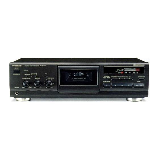
Ш FRONT PANEL CONTROLS
1
ATANDBYOION
No. Name
(1) Power “STANDBY (L/ON” switch
(POWER, STANDBY ()/ON)
Press to switch the unit from on to standby mode or vice versa,
in standby mode, the unit is still consuming a small amount of
power, |
Standby indicator (STANDBY) |
When the unit is connected to the AC mains supply, this indica-
tor lights up in standby mode and goes out when the unit is
turned on.
(3) Multiplex filter button (MPX FILTER)
(4) Dolby nolse reduction buttons
(DOLBY NR B, C)
6) Auto tape calibration button (ATC)
(6) Cassette holder
7) Tape/iinear counter reset button
(COUNTER RESET)
Tape/linear counter mode button
(COUNTER MODE)
(9) Remote control signal sensor
Memory stop button (MEMORY STOP)
M Pause button (II PAUSE)
(2) Automatic record muting button
(O AUTO REC MUTE)
e
| RS-BX501
No. Name
(3 Record button (6 REC)
Reverse-mode select button
(REVERSE MODE)
(5 Headphones jack (PHONES)
Headphones volume control
(PHONES LEVEL)
(7 Recording balance control (BALANCE)
Recording level control (REC LEVEL)
Cassette holder open/close button —
(4 OPEN/CLOSE)
@ Playback buttons (</b>)
@ Stop button (M)
@ Rewind/fast-forward search buttons
(<</>> [TPS])
RS-BX501
H ACCESSORIES
ACpowersupplycord .......... cin... 1 pc. Stereo connection cables (SJP2276) .............. 2 pcs.
(For (EB) area: VJAQ733) — (for others: RJA0019-2K)
E
>= DI)
==
IN CONNECTIONS
Before making connections, make sure that the power to this unit
and alt other system components is turned off. For (EB) area only
Note BE SURE TO READ THE CAUTION FOR AC
MAINS LEAD ON PAGE 2 BEFORE THE
e Avoid letting the cables touch each other as much as possible,
otherwise noise will be generated. FOLLOWING CONNECTIONS.
e The configuration of the AC outlet and AC mains lead differ
according to area. Placements hints
®Although the figure below shows the AC power supply cord If this unit is placed near a receiver or a tuner, a “hum” noise may
being connected to a household AC outlet, if the amplifier (or be heard during tape playback, recording, or AM reception of the
receiver) is equipped with an AC outlet, connect the cord to that receiver or the tuner. ;
outlet. If this occurs, leave as much space as possible between the
units, or place them where there is the least amount of “hum”.
Stereo connection cable
White (L) <TD AT Insertion of connector
Red (AR) mm N= Even when the connector is perfectly
inserted, depending on the type of in-
let used, the front part of the connec-
Connector
Amplifier tor may jut out as shown in the draw- Co
or receiver ing. N
H there is no problem usin Approx. 6 mm
TAPE owever here 1s p m using Appliance inlet
REC_PLAY the unit.
(OUT) (IN)
O OA
ООО
С Cn
a С
Connect this cord after
all other cables and
— | cords are connected,
: 6]
| Household AC outlet
(For (EB) area only)
/
— ir ан = — — —
AT
A
Il PLAYBACK
Either normal, CrO: or metal type cassettes can be used.
1 STANDBY
indicator
RS-BX501
ORENSE RR AAA EEE 1 € #6 6 4 6 6 4 EP 6414 ET 61 0 1 10 0 1 1 1 A EN 3 8 A 4 #31
Press POWER.
(The unit will switch on.)
Standby indicator will go off.
+ 1 + 14 + + 1 ù % 6 4 4 8 4 4 AA 0 C4 FEAF odor kok FEF EEA Edd edd
2 OPEN/CLOSE Press OPEN/CLOSE, and then
insert the cassette tape.
Press again to close the cassette holder.
Forward side Reverse side
Tape opening | Temo 1
facing downward. =
= —
}
- — 30-26-20 -16-12-10 -B <4 -4 -2000 +2 +4 +45 49
titi h
td
Г
—
|
TYPE |
The tape type will be displayed.
aaa AA 1 54 5 5 10 1 4 5 5 51 EE 5 80 4 41 A 414511 40 C1 чем ия мня нии нана
3 DOLBY NA Press either DOLBY NR Bor C
Q to select the appropriate
Q
S ^^
noise-reduction system.
(5 30-28-2018 “12-10 -5 =6 -4 -2000 +9 +4 46 4B
-—
1"
PILI
Al
[> DOLBY NA
TYPE | |
liluminates
Select the same type as that used for recording. When piay-
ing back a tape which was not recorded using a Dolby NR
system, press so that the indicators go off.
—
——
180 E A A RE
4 REVERSEMODE Press REVERSE MODE to se-
lect the appropriate reverse
—w mode.
A E r ( 30-25-20 —15-12-10 -A -8 =4 -2000 12 но но 48
our
sl
[> DOLAY NR cp
Each time the button is pressed, the indicator will change in
the order:
— : One side only.
>: Both sides repeatediy (up to 8 times).
(Refer to page 8.)
5 Press > or 4.
> (Playback will begin.)
№»: To begin from the forward side.
4: To begin from the reverse side,
4 Indicates the side being played.
Q
— Fo y 7 Cem 7 CN
“и Li ! Li AU CONTO ATAN
> PLAY PEL DOLBY HA cry
illuminates
To temporarily stop playback
PAUSE
Press HI.
I The "PLAY" indicator will flash.
Press once again to resume playback.
To stop playback
Press Ш.
For your reference:
When the cassette holder is open, pressing À, pl, << or >> will
close the holder and begin the desired function.
About the automatic-tape-select function
This unit is equipped with the automatic-tape-select feature; it auto-
matically detects the type of tape being used, and then makes the
suitable adjustments of the blas and equalizaiton accordingly.
The type of tape being used will be automatically detected and the
indicator will illuminate.
TYPE 1: NORMAL
TYPE Il: СгО:
TYPEIV; METAL
RS-BX501
About the Dolby noise-reduction system
The Dolby noise-reduction system is designed to effectively reduce
the annoying high-frequency “hissing” noise typical of cassette
tapes. During recording, the system functions to increase the high-
frequency sound level, the sound, and then, during playback, that
same portion is weakened to bring it back to the previous level.
This unit includes two types of Dolby noise-reduction systems, the
Dolby B NR-type and C NR-type.
Dolby B-type noise-reduction
Noise is reduced to about one-third,
Use this system when playing back tapes recorded by the Dolby-B
noise-reduction system, such as prerecorded music tapes, etc.
Dolby C-type noise-reduction
Noise is reduced to about one-tenth,
Use this system for the recording and playback of sound sources
that have a wide dynamic range and good tone quality, such as FM
broadcasts of live performances, etc., and for playing back such
tapes.
About the Dolby HX-Pro headroom
extension system
By functioning to improve the maximum output level of the tape's
high-frequency range, this system permits recordings without a re-
duction in the level of the sound source's high-frequency range. In
addition, by using the system in parallel with this unit's noise-reduc-
tion system, recording and playback with a greatly extended dy-
namic range is possible.
Reverse function
The reverse function on this unit has two modes (Ir , CD). Read
the descriptions below and select the mode as desired,
(Refer to step 4 on page 5.)
Mode Tape travel
Only one side of the tape (either the forward side or
———» | the reverse side) will be played, and operation will
«+-—— | automatically stop when playback has been
completed.
Both sides of the tape will be played repeatedly
eight times, and then operation will automatically
cc: stop.
(If playback is begun from the reverse side, the
forward side will be played seven times.)
H TO FAST-FORWARD OR REWIND
THE TAPE
— 7 2520-15-12 -140 -8 8 -4 —2000 472 +4 +0 18
DOLBY NA
TYPE I g E?
só 8. >
_ 00.
© |
x ] -
LU
[TPS] [In stop mode]
| Press << or >>.
+ >>
ss
= + 1 # + + EEE EEES ES ESSE ESSE ESAS ESSE EAS AAA
Because this unit is capable of playing back both sides of the tape,
the operation changes in accordance with the direction of the tape
side indicator.
Tape side Rewind Fast forward
indicator
> “4 | >>
el
<T >> +4
High-speed tape transport
When fast-forwarding from near the beginning of the tape or when
rewinding from near the end of the tape, the tape travel speed will be
faster than that during normal fast-forwarding or rewind.
(During high-speed tape transport, the (H) indication will light up.)
This high-speed tape transport will also function during TPS.
En N 4-30 20-20-16
Ei
>
(H) indication
RS-BX501
Il ABOUT THE ATC FUNCTION
The ATC (auto tape calibration) function records a test signal in
order to automatically set the bias, equalizer and recording/playback
level to the optimum recording conditions in accordance with the
characteristics of the tape being used.
The table below shows the conditions of the display and the opera-
tion of the unit while the ATC settings are being made.
O Display Unit operation
The bias is adjusted so that the output level is the
same at 400 Hz and at 10 kHz.
"BIAS" is displayed.
Output level (dB)
+
<=
1 0 £
, , 11D Cee A / 400 1K 3K 10K Frequency
(1) Bias adjustment Bins, queje (Hz)
< тих QE [ATOHENORY—
il
Flashes fa 1
. 4
=
*
=
“
le.
bl
LY
“
+»
-
>
“
+
LS
Na
*
o
2
D
>
QD
"EQ" is displayed. =
| 2
6
: . a N 0
© Equalizer adjust- L y Ast unas pan 400 1K 3K 10K Frequency
ment <<] pay [— ATO MEMORY — = / + < 5 7 (Hz)
Flashes
The equalizer is adjusted so that the output
level is the same at 400 Hz and at 3 kHz.
mo
=
©
“LEVEL” is dispalyed. 2
=
| | g Frequency
о DEC diem ино о (Hz)
® Level adjustment nO UT / 400 1K 3K 10K
<] PLAY p — ATC MEMORY — = o A |
X
/ 1
+ 1
r
Flashes
The tape sensitivity is compensated so that
the recording input level and the playback
output level are the same.
RS-BX501
IN SELF-DIAGNOSTIC
Indicating Procedure
Indicating Position
| To indicate Self-Diagnostic Function |
1.
2.
7.
8.
Check the cassette holder is empty (no cassette tape),
then turn on the power.
Press and hold the DOLBY NR B button (for more than
3 seconds), and also press the STOP (IB) button for
about 2 seconds until the level meter changes from
constantly lit to blinking.
Insert a normal blank cassette tape, either A or B side
of which has the erase preventing piece folded. Then
close the cassette holder.
Press the FWD. PLAY (Pp) button and play the tape for
more than 1 second, then press the STOP (IM) button.
Insert a normal blank cassette tape, both A and B
sides of which have the erase preventing pieces
respectively, and close the cassette holder.
(NOTE: Rewind the tape for 1 or 2 minutes before use.)
Press the REC (0) button.
This automatically makes Deck perform the following
operations.
[DOLBY B NR | REC
<
= eE 8 SS = xs =
o i 5 5 ED 5
- 26086 OE
©
Self-Diagnostic Function indication
STOP | FWD. PLAY |
(Example)
>
LI 4 O rennrantiaoDoccarterent
LO |
-M-2-20-15-12+ & -6 74 -2000 +2 +4 18 48
¡Record an eight second portion with no sound. | > | Record a 20 second portion off 400Hz test signal. |
[When the signal is detected, stop the unit| 4m |TPS-REVIEW search mode |4m|Stop the unit]
(NOTE: The tape has to be taken up by playback for about 1 minute.)
To check the self-diagnostic results, press the STOP (IM) button.
These results are indicated in the respective displays.
If there is no fault, the counter display remains unchanged when the STOP (Il) button is pressed.
| To resume Ordinary Indication |
To return the display to normal mode, switch the power off and then back on again.
To have the indication appear again, take the above-stated steps 1, 2 and 8.
NOTE: The self-diagnostic results are stored in memory.
To clear this memory, press and hold the STOP (IM) button for at least 6 seconds until “CL” appears in the
FL dispiay.
Be sure to clear the memory after the repair.
Indication Text
Symbol Trouble Remedy
irregular action of cassette mechanism. The cassette mechanism mode switch (5971) and plunger
Ho (Example) Pressing the FWD PLAY button results in REW are defective.
PLAY action. (Check and replace them.)
No recording can be made, or the unit is placed in the The erase preventing switch (S974, S975) contacts
Ног recording mode though the erase preventing piece has improperly, or there is a shortcircuit. |
been broken. . (Check and replace the switch.)
Pressing the PLAY (>) button fails to play the tape. The cassette half detect switch (5972) contacts
HO3 Pressing the PLAY (p>) button causes the motor to rotate | improperly, or there is a shortcircuit.
though no cassette tape is in. {Check and replace the switch.)
HO4 The cassette holder will not open or close when the The cassette holder open/close detect switch (S853,
OPEN/CLOSE (A) button is pressed. 5854) contacts | ; .
improperly, or there is a shortcircuit.
HO5 Pressing the OPEN/CLOSE (A) buttton causes the (Check and replace the switch.)
cassette holder to open after it has closed, and vice versa. p -
The auto tape select (CrO,) switch (5973) contacts
H06 No treble is produced when a normal tape is played or improperly, or there is a shortcircuit.
recorded. (Check and replace the switch.)
Excessive treble is produced when a CrO,/Metal tape is - -
played, or the recorded treble is destorted and at a low The automatic tape select (Metal) switch (S976) contacts
НО? level. improperly, or there is a shortcircuit.
(Check and replace the switch.)
When the PLAY (D>) button is pressed, the tape runs a little The hall IC (1C971, 972) is defective and, as the result, reel
FO1 and stops soon pulse is out of order.
p ; (Check and replace the IC.)
| The PLAYBACK AMP IC (IC2) is defective.
FO2 TPS dose not operate. (Check and replace the IC.)
RS-BX501
IN DISASSEMBLY INSTRUCTIONS |
ll OPERATION CHECKS AND MAIN COMPONENT REPLACEMENT PROCEDURES
1. This section describes procedures for checking the operation of the major printed circuit
boards and replacing the main components.
2. For reassembly after operation checks or replacement, reverse the respective procedures.
Special reassembly procedures are described only when required.
3. Select items from the following index when checks or replacement are required.
4. lllustrated screws are equivalent to actual size.
5.[ ] indicates parts No.
e Contents
page.
1. Checking for the FLP.C.B. * * + + + + + + = + a 000000006000 000000000000 00 + 10,
2, Checking for the operation P.C.B. + «+ < + + + ++ 000000000000 00000000 0000000000 11.
3, Checking for the main P.C.B. + + + + + ++ 0 + a 0000000 00000000 0000000000 12,13.
4. Checking for the motor P.C.B.+ + + + + + + +000 000000000000 000000 0000000000 13,
5, Replacement for the mechanism unit. * < + + + + < ec vs 0 000 0020000000000 14,
6. Replacement for the head block (R/P) and pinch roller ass’y. * e « «e ¢ se sc sv 00 000000 15,16.
7. Replacement for the belt, flywheel ass’y, reel motor and capstan motor, ¢ + << + » ¢ = © ¢ +o © ¢ 16,17.
8. Replacement of the parts mounted on mechanism P.C.B. and the plunger. « + » » + ¢ oc os ¢ co 17,18.
9. Replacement for the drive rack and friction gear, « = ¢ ss ss ces 0s ss 000 ps0 000000 18.
1. Common disassembly procedures
(Follow this procedure prior to other disassembly.)
Cabinet [RKM0036- K]
SCRE Remove the 6 screws.
(5 ju 0060
(RHD30035-K] (Black)
VID ee
(XTBS3+8JFZ1) (Black)
RS-BX501
2. Checking for the FL P.C.B.
ETD Follow the disassembly procedure described
in item 1 on page 9.
“ei
FL P.C.B.
(Solder side)
SCHE] Remove the connectors. CEE) Remove the 4 screws.
Front pane! ass'y [RFKGSBX501EK]
CN2B
CP1
CN3B
SL Remove the 6 screws and connector.
FL P.C.B.
(Component side)
Ey» 0-0
XTBS3+8JFZ1) (Black)
Em 6-0
(XTBS26+8J)
Remove the FL holder piece.
RS-BX501
3. Checking for the operation P.C.B.
Follow the disassembly procedure described
in item 1 on page 9.
EEX) Remove the connectors.
CN2B
ED Remove the knobs and nuts.
Knobs
[RGWO177A-1K] Nuts
[RHN90001]
f Operation P.C.B.
(Solder side)
Remove the 4 screws.
Front panel ass'y [RFKGSBX501EK]
CP
CN3B
E» 0-0
(XTBS3+8JFZ1) (Black)
mm 0-0
(XTBS26+8J)
©
Operation P.C.B. |
(Component side) (RHD26016)
RS-BX501
4. Checking for the main P.C.B.
EXD Follow the disassembly procedure described
in item 1 on page 9.
EEX Remove the 4 screws.
9
= ©
Г
Л
» O
©
Power transformer
ce, N
=
AN
»
[wy
//
SIGE Remove the 5 screws,
Main P.C.B.
à Main P.C.B.
(Component side)
Remove the 5 screws.
ES Install the power transformer on the main P.C.B.
and power supply P.C.B.
Main P.C.B,
00
® INDIO 0-0
XTB3+20JFZ) (Black)
Y) DD 0-00-€6
XTBS3+8JFZ1) (Black)
RS-BX501
EXI Install the rear panel to the main P.C.B.,
power supply P.C.B. and power transformer
With 4 screws,
Rear panel
Main P.C.B.
(Solder side)
5, Checking for the motor P.C.B.
Follow the disassembly procedure described
initem 1 on page9. °
ST Remove the connectors.
CN2B
CP1
CN3B
EXD) Unsoider the reel motor and capstan motor terminals.
So Remove the 2 screws, claw and connectors,
Motor P.C.B.
(Solder Side)
Step 3
Remove the 4 screws.
Front panel ass'y [RFKGSBX501EK]
o CP852
1/
Reel motor
Ccapstan motor
terminals
terminals
) Sa
Handle the connector with care
so that the shape of terminal is
different from others.
Claw | E O | ti
Or о — Е |
| | - Motor P.C.B.
pe
Го — CN52B
Gp 0-0
(XTBS3+8JFZ1) (Black)
Jm 0.6
XTW2+6S) (Black)
RS-BX501
6. Replacement for the mechanism unit
ETF) Follow the disassembly procedure described
in item 1 on page 9.
EXD Remove the connectors.
CN2B
CP1
CN3B
Push the drive lever and open the cassette
holder ass'y.
Drive lever
ED Remove the 4 screws and connector,
Mechanism unit
CN502 X | ÿ
Remove the 4 screws.
Front panel ass'y [RFKGSBX501EK]
Lift the cassette lid in the direction of arrow O),
and remove it in the direction of arrow O.
Cassette {id [RYF0266- К]
YI 0-0
(XTBS3+8JFZ1) (Black)
© 0-0
(XTB3+12JFZ) (Black)
RS-BX501
7. Replacement for the head block(R/P) and
pinch roller ass’y
Follow the disassembly procedure described
in item 6 on page 14.
Pull out the rivet in the direction of arrow @ while Push the drive lever and open the cassette holder
pressing the claw in the direction of arrow D. ass'y.
"A
Du, |
и Drive lever
Rivet O
Rivet
[RMQ0430]
1 J Cassette holder ass'y
EXD Overato the cassette holder ass'y in the direction (ETE) Locate the cassette holder ass'y and mechanism
of arrow, and then remove it from the boss of drive unit at a 90 degree angle as shown below, and then
lever. pull the cassette holder ass'y. |
Pinch roiler(R) ass'y
[RXP0053]
Pinch roller(F) ass'y
90°
Boss of
drive lever
Head block(R/P)
[RXQ0316-1]
Installation of the cassette holder ass'y after replacement
Locate the cassette holder ass'y and mechanism Push the drive rack in the direction of arrow.
unit at a 90 degree angie, and then install the
cassette holder ass'y.
Mechanism unit
Drive rack
Fig. 1 Cassette holder ass 'y
RS-BX501
CEE Close the cassette holder ass'y in the direction ESD Insert the rivet to the hole of cassette holder ass'y.
of arrow.
Cassette holder
ass'y
Rivet
Hole
Rivet
Claw of rivet
Ne J
8. Replacement for the belt, flywheel ass’y, reel
motor and capstan motor
Perform the SERED ~ in item 7 on page 15.
(109 Push the drive rack in the direction of arrow (1).
SED Remove the 4 screws and connector holder. CE) Remove the sub chassis ass'y.
„=
„ ne
„” >
/ `
/ Connector holder “
/
Belt
[RDV0015]
Flywheel(R) ass'y
[RXF0047]
: EH “===! 3% Push the claws in the direction
of arrow ©, and then remove
Y the connection holder in the
@ © direction of arrow O). Fiywheel(F) ass'y
[RXF0040]
ED Remove the 4 screws.
e 0600
o 7 “ Sub je ass'y
57 Ne |
Ie © © ©
zz |
Capstan motor , à > С
[ВЕМооз6-1] | o mm @ пи» 0.6
— Real motor (XTW26+125)
O O
OL 9 0.0
axl] | (XTW26+6L)
9 SN
QQ
Om 60-0
(RHD26013)
RS-BX501
Installation of the sub chassis ass'y after replacement
EEX) Place the idler gear in the center as shown below. Temporarily sevure the belt as shown below.
er ge
ar
Reel gear(B)
idl
Reel gear(A)
LL Boss(A)
| H Bei
> Boss(B)
ое] co
SE Push the drive rack in the direction of arrow. - FWD side flywheel ass'y
Install the sub chassis ass'y to the chassis ass'y
with 4 screws.
CTA) Secure the belt with the capstan motor pulley.
Belt Belt
a a
€ ==
—
К
Li
a]
N Connector holder ; Tweezers Capstan motor
NY
—
9. Replacement of the parts mounted on
mechanism P.C.B. and plunger
Perform the GE - in item 8 on page 16.
Remove the 2 screws, and unsolder the terminals |
(2 points), and then remove the mechanism P.C.B. Release the 4 claws, and then remove the dressing
plate,
Unsolder A
the 2 points
Dressing plate[RGK0582-K] Oum 00
(XTW2+65)
RS-BX501
EXE) Release the 4 claws. NOTE
Notice for Installing solenoid. Solenoid
® The shaft of solenoid
should be aligned with
the slot of lever.
TT TT ~Shatft
Solenoid [RSJ0003]
10. Replacement for the drive rack and friction
gear ass'y
EXD Perform the CED ~ in item 8 mm =
on page 16.
ETE) Remove the friction gear ass'y.
Friction gear ass'y [RXG0037]
e === === A Eee мне EE EEE ERA EE EH Eek seer
ETP) remove the drive rack using the screwdriver
inserted into the hole.
|
| i
ETE) Remove the screw and shield plate. ) }
{ !
EXI) Force the drive rack in the direction of arrow. | ore ack у, !
| I
o | |
| |
Shield plate | qu ——- + — |
|
a | l
| i
e o O | Claw of chassis |
J) Emr dE dm —— кн mm mm сте mm === == => es dpe mk eh Bed ME Ml ME EE EE Em EEE de == == A de —
Drive rack —] J
[RMQ0312A] o
,
@—
pS
A Drive rack ‹
mm ©
(XTW2+65)
RS-BX501
Hl WRITING TO EEPROM
This unit is equipped with EEPROM memory that stores a variety of design data and performance data
such as piayback gain, bias value, recording gain, recording equalization, etc., which was programmed
at the factory. a
This EEPROM memory is capable of being read and written to more than 100,000 times. To illustrate
this, if one ATC operation is performed every hour continuously every day for ten years, it world still be
possible to successfully read and write with the EEPROM. |
Data is actually written in this EEPROM only when ATC is actuated or when power supply is turned on or off.
Since it hardly breaks down, there will scarcely occur such a trouble as to require replacement.
Measurement Condition
¢ Recording-level control; Maximum * Headphones volume control: Maximum
* Recording-balance control; Center | .. *Make sure heads are clean
e Reverse-mode selector switch; = * Make sure capstan and pressure roller are clean
e Dolby NR switch; Off * Judgeable room temperature 20+5°C (68 £9°F)
* ATC switch; Off
Measuring instrument
* EVM (Electronic Voltmeter) * ATT (Attenuator)
® Oscilloscope - e Resistor (6000)
* AF oscillator
NOTE: Before adjustment, be sure to set the AF oscillator output level to OdB (1kHz): 1 Y
Test tape
e Playback gain adjustment (315 Hz, 0dB); QZZCFM
e Overall gain adjustment and Overall frequency response
Normal reference blank tape; QZZCRA
CrO; reference blank tape; QZZCRX
Meta! reference blank tape; QZZCRZ
NOTE: Step 2 to step 7 only has to be done after exchange of the EEPROM.
Step 1 Short the Test Mode terminals with a shorting clip (see Fig. 1).
Y
Step 2 While holding down the STOP button on DECK2, press the POWER A
Р switch to ON. | J’
J
All FL display segments except for the four-digit counter on DECK2 Short clip
will start blinking to indicate that the deck has entered Write mode.
At this point the four-digit counter will indicate “00”. =
Step 3 pm SS msm em mm mm me > |
77) г) гу | 98-30—25—20—15-12-10-8-6-4-2 00 0+2+4+6+8) Fg. 1
LI LI LI EI Y + | Notes:
AN == LL 0 0 0 re e * The test mode terminals
7 on main P.C.B. should be
Blinks shorted with a short clip
as shown above figure.
* After the adjustment
items disconnect the
short clip.
RS-BX501
Step 4
Step 5
Step 6
Step 7
Step 8
©
'
The counter shows a four-digit hex number. The two high-order digits
indicate a ROM address, and the two low-order digits indicate the data
stored at that address.
L set these digits using the REC or
PAUSE button. The high- and
low-order digits of the data
increment alternately each time
the REC button is pressed. The
PAUSE button causes these
set these digits using the FF or
REW button.
The high- and low-order digits
of the address increment alter-
nately each time the FF button
is pressed. The REW button
causes these digits to decrement digits to decrement alternately.
alternately. For fast incrementing or
For fast incrementing or decre- decrementing, hold down the
menting, hold down the FF or REC or PAUSE button.
REW button. |
Y
Begin from address 00 and write data up to address 7F (data in
[ 1). Check that the data at address 7F is “00” (end), and then exit
the write mode.
'
restore the normal Test mode. The four-digit counter on DECK1
displays.
po a > > == LL = = = = Z—>
|! dB—30—25-20-15—12-10-8-6-4-2 DC 0+2+4+6+8)
After completing ROM writing, press the STOP button on DECK2 to
PLAYBACK GAIN ,
*Set the AF oscillator's output frequency to 315Hz/—20dB (100mV)
(see Fig. 2).
¢ With no tape loaded in the deck, press and hold the REC button.
Adjust the test signal level using the Rec. Level and Balance controls
until the line output levels on both channels are 320mV. When the
adjustment is complete, release the REC button. (The deck stores
the data at the moment the REC button is released.)
* Load the test tape, QZZCFM, into the deck and locate the section of
the tape where the playback gain test tone (315 Hz, OdB) is recorded,
then playback the portion. Press the ATC button, and the display will
flash —ATC MEMORY — slowly, meaning that playback gain is being
automatically adjusted. Press the FOW. PLAY button. (At this point
the deck automatically adjusts playback gains.) After this play back
the tape and verify that the output level falls in the specified range.
Standard value: 320mY +0.5dB
Note: If adjustment of PLAYBACK GAIN fails, the display will flash
— ATC MEMORY — rapidly. After a successful adjustment, the
display will no longer show —ATC MEMORY —.
Example: Set “FF” in address 03
(see Fig. 3).
Lose these digits to
“5A” using the
REC or PAUSE
button.
_ Set these digits to “03”
using the FF or REW
button.
* The data writing process is
complete when the next
address number appears.
For example, writing of the
data 03.5A has been
completed when the
address 04 is displayed.
|
©
N Ё LINE Qui
LINE IN 7
©! = = = а === todo
но ГОО kn o TT IO),
EVM
Fig. 2
INITIAL SETTING UP FOR OVERALL GAIN
AND OVERALL FREQUENCY RESPONSE
Step 9
Step 10
eLoad a Normal blank test tape (QZZCRA) into the deck under test.
Press the ATC button, then the REC button. The display will flash
— ATC MEMORY — slowly. (At this point the deck automatically adjusts
the overall gain and frequency response.)
* After the above setting, the overall gain for selection of CrO, and Metal
tape will be automatically set by the ROM and stored in the ROM.
Note: If adjustment of OVERALL GAIN or OVERALL FREQUENCY
RESPONSE fails, the display will flash — ATC MEMORY — repidly.
After a successful adjustment, the display will no longer show
— ATC MEMORY —.
À
Remove the shorting clip from the Test Mode terminals. The FL dispiay
will stop blinking.
RS-BX501
Note: If the microprocessor is replaced, it is not necessary to replace (or write data to) the EEPROM.
« EEPROM MAP
Note: At an address with no data value indicated (e.g. 01 — —), the ROM operates
Вне 1 2 3 4 5 6 7
0 00 — — — — — — —
1 — — — — — — — —
2 — — — — — — — —
3 5A — — — — — — —
4 — — — — — 68 84 90
5 — — — — — 78 60 60
6 — — — — — 38 30 | 18
7 — — — — — 64 68 78
8 — — — — — AS BO 8C
9 — — — — 94 — — —
A — — 6A OF — — — —
B — — 70 2B — — — —
с — — 4B 12 — — — —
D — — 72 07 — — — —
E — — 40 | FB 00 70 74 04
F — — 53 F5 00 — — 00
Fig. 3
normally irrespective of the kind of the data supplied.
RS-BX501
HB MEASUREMENTS AND ADJUSTMENTS
Measurement Condition
e Recording-level control; Maximum * Make sure heads are clean
* Recording-balance control; Center | * Make sure capstan and pressure roller are clean
* Reverse-mode selector switch; = e Judgeable room temperature 205°C (68+9°F)
e Headphones volume control; Maximum
* Dolby NR switch; Off
* ATC switch; Off
Measuring instrument
« EVM (Electronic Voltmeter) * ATT (Attenuator)
* Oscilloscope * DC voltmeter
* Digital frequency counter * Resistor (6000)
* AF osciliator
NOTE: Before adjustment, be sure to set the AF osciltator output levet to 0dB (1kHz): 1Y
Test tape
* Head azimuth adjustment (8kHz, —20dB; * Tape speed adjustment (3kHz, —10dB); QZZCWAT
+ Playback frequency response (315 Hz, * Overall gain adjustment and Overall frequency response
12.5kHz, 10kHz, 8kHz, 4kHz, 1kHz, ; QZZCFM Normal reference blank tape; QZZCRA
250 Hz, 125 Hz, 63Hz, —20dB) | CrO, reference blank tape; QZZCRX
* Playback gain adjustment (315 Hz, 0dB) Metal reference blank tape; QZZCRZ
* Adjustment Points
Tape speed
MOTOR P.C.8.
Short Ctip
Notes:
* The test mode terminals on main P.C.B. should be
shorted with a short clip as shown left figure.
* After the adjustment items disconnect the short clip.
RS-BX501
HEAD REPLACEMENT
When replacing the head, adjust the head azimuth as instructed below, and rewrite the data to the EEPROM.
(By adjusting head azimuth, data is automatically written to the EEPROM.)
(1) (2)
| Step 1 on page 19 — Step 8 on page 20 |
(4) (3)
| Step 10 on page 21 < Step 9 on page 21 —
(The adjustment is necessary because the playback gain, the overall gain, and the overall frequency response are
changed by the head replacement.)
HEAD AZIMUTH ADJUSTMENT
1. Playback the azimuth adjustment portion (8kHz, —20dB)
of the test tape (QZZCFM). Vary the azimuth adjusting screw
until the output of the R-CH are maximized.
. Perform the same adjustment in the play mode.
. Repeat the same check in reverse play mode.
. After the adjustment, apply screwlock to the azimuth adjust- | E. HEAD R/P. HEAD
ing screw.
о o
o @Rch a
MU mw ow — 6
A GO M
=== тоны кт "===
Lt
o
o
LNEQUT 4-49; mf
(Playback) EVM Azimuth Screw Azimuth Screw
(Forward) (Reverse)
Fig. 4 Fig. 5
TAPE SPEED ADJUSTMENT
1. Playback the middle portion of the test tape (QZZCWAT).
2. Short the test terminal. LINE OUT
3. Adjust VR853 so that the output is within the adjustment / mn
target. ° A ==a —Lo*
o o pa oO
Adjustment target: 3000 +15 Hz gia frequency
counter
Fig. 6
PLAYBACK GAIN MEASUREMENT
1. Short the test terminal. LINE OUT =
2. Load the test tape (QZZCFM) into the deck and locate 7
the part where the playback gain test tone (315Hz, 0dB) is | © eS kt: Br
recorded. After this, play back the tape and verify that the 9_o —
output level falls in the specified range. EVM
Fig. 7
Standard value: 320mY +0.5 dB
3. Release the test terminal.
4. When the data is not within the specified range, the head azimuth should be readjusted as instructed below and the
data in the EEPROM rewritten. (By adjusting head azimuth, data is automatically written to the EEPROM.)
When adjusteing head azimuth, check the test tape for scratches or crease. If any exist, use a different tape and
follow instructions 1 to 3 below.
(1) (2) (3)
Step 1 on page 19 el Step 5 on page 20 He Step 10 on page 21
RS-BX501
PLAYBACK FREQUENCY RESPONSE
1.
Playback the frequency response portion (315Hz, 12.5kHz—
63 Hz, —-20dB) of the test tape (QZZCFM).
2. Assure that the frequency response is within the range
shown in Fig. 9 for both L-CH and R-CH. -]+5dB
E+
008
—2dB
LINE OUT — 3dB
/ СЛ — 508
o hana ==3 Fedo
ос ©); 63Hz 100Hz 200K 500 H2 1kHz 2kHz 4kHz ;
EVM
ERASE CURRENT MEASUREMENT
1. With no tape loaded in the deck, press the Record button. x
2. Check if the output at this time between the erase current a
confirmation point TP1 and GND (chassis) is within the +
standard value. ERASE HEAD EVM
R308 10 (Electronic
Standard value: 190 + 25mA (Metal)..EVM Reading: 190+25mV Voltmeter)
Fig. 10
CONFIRMATION OF THE OVERALL GAIN AND OVERALL
FREQUENCY RESPONSE
1.
In the Record Pause mode, load a normal blank tape (QZZCRA)
into the deck, and apply the reference input signal (1kHz,
—24dB) to the Rec. input. Adjust the output to 320mV with
the attenuator, and start recording.
While playing back the reference signal just recorded, verify
that the output level fails in the following range.
Standard value: 320mY +0.5dB
Afterward, apply a signal (frequency at the measured point in
the range from 50 Hz to 10kHz), whose level is 20dB lower than
the reference signal level (1kHz, —24dB=approx. 63mVj}, to
the Rec. input. Then start recording with a normal blank tape
(QZZCRA).
Play back the test signals just recorded and verify that the
levels at the test frequencies fall in the ranges specified in
Fig. 11 with respect to the reference signal level.
Repeat steps 3 and 4 above for CrO, blank test tape (QZZCRX)
and Metal blank test tape (QZZCRZ), in these cases raising
the upper end of the test signal frequency range to 12.5kHz.
Verify that the signal levels at the test frequencies fall in the
ranges specified in Fig. 12 with respect to the reference
signal level.
Steps 1 through 2 above are concerned with overall gain;
steps 3 through 5 pertain to overall frequency response.
Normal Overall frequency response chart (NR OUT)
+648
+406
+2
+408
0dB
—2
—4
— 308
5OHz 100H: 200H:z 1 2kHz
Fig. 11 |
CrO, Metal Overall frequency response chart (NR OUT)
10kHz
+6dB
+4d8
+
~3+5dB
bai
—2
—4 — 408
S0Hz 100Hz 200Hz 500Hz 1kHz 2kHz 12.5kHz
Fig. 12
“ LINE IN LINE OUT
oTE
a?
AF oscillator ATT
Fig. 13
When the data is not within the specified range, the head azimuth should be readjusted as instructed below and the
data in the EEPROM rewritten. {By adjusting head azimuth, data is automatically written to the EEPROM.)
When adjusting head azimuth, check the test tape for scratches or creases.
follow instructions 1 to 4 below.
If any exist, use a different tape and
If outside the standard value, data in EEPROM should be written again by taking the following procedure and there
thereafter section 1-6 should be carried out again.
(1) (2)
(3) (4)
Step 1 on page 19 — Step 5 on page 20 |-> Step 9 on page 21 | Step 10 on page 21
Checking Method” on page 31.
The unit is not turned on.
Te.
oz
/
Hl TROUBLESHOOTING GUIDE
* To perform troubleshooting, set the unit to the state described in the “Motor Control PCB
Power switch turns on but
mechanism does not operate.
Voltage check:
Approx. 5V at GN52B pin 1
Approx. 7.5V at CN52B pin 3
Approx. 15V at CN52B pin 2 al
CN2 pin 13
| OV (ground) at CN52B pin 12 a
CN2 pin 10
YES
“6
Y
Check switches in the self-
diagnosis mode (see page 8).
Y
Any switch is not failure stored
memory ?
YES
OPEN/CLOSE does not operate
correctly.
YES
Y
The voltage is not output at Q608 NO
emitter approx. 5.6V ? A
YES r
r When the POWER button is NO
The voltage across R624 is less NO on/off, the voltage at Q603 base
than 16V change from 5V to OV
| respectively.
YES YES
Y y
R624 replacement. When the POWER button is
NO on/off, the voltage at pin 17 of
CN3A and CN3B changes from
5 Y to OV respectively.
YES
The voltage D614 and Q608 base | NO N Connection checks for
is less than 6.2V Ce connectors, FFC cable,
soldering, etc.
YES
i
D614 and Q608 replacement.
Does the voltage hy ao to NO _ | Q603 soldering check or _
cos or change from "| replacement. >
YES
A
Does the voltage at Q604 NO
collector change from —20V to æ| Q610 and —20V system check. >
15V?
YES
Y
Does the voltage at D613 change NO ‚| D613 soldering check or N
from OV to 8.2V ? | “| replacement.
YES
Y
NO
Does the voltage at Q605 emitter
change from —0.4V to 7V ?
YES
Y
Power is normal.
R622 disconnection, or Q605
check or replacement.
Unplug the power cord and fort
the door to the half-open positic
by hand. :
The door does not close when tr
power cord is plugged in again,
check door switches S853 and
S854 are in the off positions.
YES
у
Does the voltage at CN52B pin 1
change when the door switch
(5853 and S854) is forced into th
on position ?
YES
d
Does the voltage at the
microprocessor pin 62 terminal
also change ?
YES
J
To the microprocessor check
section.
NO
|
» Connection and power check.
_
|
_
NO
NO Replace any failed switch with a
new one.
Both power and microprocessor
NO
е
2
№
e
NO
“| system are normal.
Switch is failure.
LH LL
Check connection between the
motor PCB and the sub PCB.
Y
RS-BX501
Does the flywheel turn instantly |
when the AC cord is plugged in ?
YES
Y
Force the mode switch into the
on position for more than a
second.
Does the head lift once and then
lower ?
NO
YES
Y
Does the plunger instantly pull
YES
in?
NO
YES | Are power and connection
|
checks normal ?
NO
To the microprocessor check
section.
i
Power is failure.
RS-BX501
Microprocessor check section
|
Is the voltage at Microprocessor NO
pin 57 approx. 5V ? ] » Connection and power check.
YES
Y
Is the voltage at Microprocessor NO N
pin 60 approx. 5V ? “
YES
/ =
Is the voltage at Microprocessor | NO
pin 24 OV ? “
YES
Y
Is the voltage at Microprocessor NO
pin 59 OV ?
YES
Is the clock oscillating ? NO
(check with an oscilloscope and че
1:10 probe.)
YES !
| "NO | There are no pulses at
-— —— microprocessor pin 21 and CN3
pin 12 ?
YES
Check power, D601 and D602
circuits and their connections.
audio circuit
Does failure occur in audio
circuit or tape mechanism ? » To the audio circuit
tape mechanism
Y
To the tape mechanism.
RS-BX501
Tape mechanism
that order.
» 10501 0, ©
The voltage does not input to AD
change as each operating switch
is pressed ?
NO
Voltage increases from OV
in approx. 0.4V
increments when Stop, F.
Play, R. Play, FF and REW
buttons are pressed In
YES
Check continuity of switches
whose voltage does not change
when pressed.
in case of fallure, replace with
new switches.
Tape mechanism 1
Does the voltage at
microprocessor pin 62 and 64
change when S801 and S802 of
the mechanism PCB (or the leaf
switch of the mechanism) are
forced into the on positions ?
NO
YES
Does similar pulses develop at
CN1 pins 4, 5 and 6 of mechanism
when the mode switch is pressed
on ?
YES
Y
Are pulses applied to terminals
13, 15 and 16 of 1C852 when the
mode switch is pressed on ?
NO,
YES
Y
Do pulses develop at
microprocessor pins 26, 27 and
28 when the mode switch is
pressed on ?
NO
Connection check for Connector
switch is failure.
Soldering checks
YES
i
Does the plunger pull in Play
button is pressed instantly ?
NO
Y
Y
Microprocessor is failure.
YES
Y
Does the plunger remain pulled in
during FF/REW operatlons ?
YES
J
Belt has come off.
Reel motor failure.
10852 is faliure.
NO
Plunger is failure.
Q854, Q804, D802, 0852, D854,
D804 fallure.
10852 15 failure.
Audio circuit
1
Does the voltage change at 1C152 | NO
pin 12 when in the REC and Stop IC152 Is normal.
modes ?
YES
Y
Do pulses develop at
microprocessor pins 20 and 21 NO
when REC mode changes to Stop
mode
» Microprocessor is fallure.
YES
Y
Do puises develop at 1C152 pins | NO
2 and 3 in the REC and Stop
modes ?
| Connection checks for
"| connectors, FFC cable.
YES
Y
IC152 Is fallure.
As shown above, check the voltage at each pin of 1C152 for the following:
MO Equalizer 120us/70us change.
®@ Dubbing seed does not change.
O Erase current does not change between the CrO, and Normal/Metal tape.
(Erase current for CrO, and Normal tape Is the same.)
@ Deck 1 and deck 2 produces no change.
O) Dolby off, B and C produces no change.
® REC and Play produces no change.
@ Auto REC mute does not operate.
Hl BLOCK DIAGRAM
ANT384N-SG
Les)
ELECTRIC YOLUME
IS 13
HEC (IN) [ }
tL cht
06,7
À control
Buffer Rec leve!
caniral
Q8
(Go
Vref
Vee
VR7O2
(BALANCE)
46, 70
Rec blos
control
VRTOI
IREC
LEVEL]
AN73525-E2
PLAYBACK AMP
Г
17
Je:
ono |
RP
———— = —
—_——, — — — — X1/X2 |
|
12047 0h
DD
27
2)
L
в
03104)
Head
select
{Play.an)
R/F HEAD «—=
ILchl
AN73535"E2
REC EQ AMP
(L302}
0304
14
15)
3 7
16} t12 UN
UPCI297CA
DOLBY HX PRO
Absolute
det YCA
т
|
ed
det
on
ti
Comporator circuit
tator
— ed
0301
Reguiotar
Bios OSC
ERASE HEAD x control
BA4S6OFTI
0302-3068
— 30 —
ANT3546C-É2 _ a - ь PLAYIQUT}
© Ÿ tL ch}
M3218 AL
DOLBY B/C NR
YA T24 Re
| IPHONES Haadphenes HEADPHONES
+ LEVEL) P-
3
О) 1612)
| i M38i23M4105F
ICH
MICRO COMPUTER
— N К PL
0 Rect | — > By" POWER
3 - o > | 1502 >
À
TT
~~] REMOTE SENSOR © VREF
Y ss | HLS LLS yen an |
< > |
| a REMOTE
137 as Т26 [25 za [es | T= : CI
(6) {CM - (7) |t18) [tien [1200 | acdl
52
+ + |
ТТ $701-718 à. pu}?
| .
DIT = 4 ' NN
— S— Pig ol
0401,403,405,L401 | | Y
MEX |(0402,404,406,L402) KEY 2
>
=
TIFT
OMT X OUT
osc
Lows)
о]
Vis
Ass
JL ILL
o
Le
XLU2040F-T2 [A Y SOT
=a B SELK ECS
DATA CONTROL L aso less ECLK {2
r-—-— ABC Rest 19 EDAT
A ENC a 06 signol te ESET
B AUTO 53 on DATA = | genergior |
с B/C 04 06 |
RO 3
D 97 CLK >
Е 120/70 9} 95 rer dû
MPX _ 6404 Vas | | . | 63
PBADJ 8 RPS
MGAIN 7 16
3 Yoo
LFADJ el „©
m
»|7
2
4 +4 4
HE
>
[ee o
So
|
|
|
|
a
METER L
IMETER R) 113}
en
N
+
>
=
»
1
|, MEZ352FPE|
(2) .
| Ich D/A CONVERTER
| Dona |
- cone
GPB-LERI VELIOS hon Lp E
Teh "
+ AOIO мес 0 (+В)
sp |
e 405 voo YO | |
GREG-L{R} y 408 | ! 26
“TE A07 (4061 | я | al
Vss MODAT$ —
BLAS LIRI a NOlZLAOI) onp $22 | 28
e | MCLK
| |
|
| RS-BX501
Notes.
1) ( } Indicates pin No. of right channel.
2)
| —9— : PLAYBACK SIGNAL LINE |
| = ¡ RECORDING SIGNAL LINE |
J
702,703
STANDBY)
i DEY
driv @ 5
drive =
a
FL5QI
FL OISPLAY
2501
mr =
|
D
XL JIBLCAGAFE
EEPROM
cs Ver Ne (+В)
mo
RVSGP25248¢
1 O)= =a, =m
| PHOTO INTERRUPTER
0601,602
FL
drive
O13
Li
N
à D1S2 D601,602
0150
Co» к —é4—
0603,604
.. a= ь
| 297) Ed 4 [LT |
BT m 3 —. $971 (MODE) “0608 D614
|} Lodder Ta S974 (R.AEC.INHI -
Энни Te er S——Pesar] ——
GB resister 15 $972 (HALF | +8) Reg
TT - Q612 -
тво!
: #85
= та 5975 {F.REC.INH} (+В) || =
| ы
Ladder 34 5 5973 ¡ATS/Cr0z] | us
CB) 4 er SL S976 (ATS/METALI] — 5 ac In
7 resister Ye 5853(0PEN DET) | об! TE 0605-608 6
Г E _— 5834(CLOSE DET.) Power q
' Ga) supply x
BAGZ26SFP-El = x
=
2
MECHANISM CONT. $ 9605,0613 — ©
Г (+8) —{ Aeguorer | ——y
7 1 D854
(PL) Ive _
> 0854 = pele
(PLidrive drive и
Ca) 23 - | SOLENOID ™ Switching
[J
244 Reel
motor | REEL
| drive 3 MOTOR
|
= Copaton, своб, бот
motor
2) 170 arive
expander Capston. 9610 #
2 , La] motor speed CAPSTAN
speed MOTOR
control | | control 0609,0613 воз
L A o e TICA
VvRBS3 Y osio
(TAPE SPEED ADJ.)
RS-BX501
3 L 4
MOTOR
CIRCUIT
Pe
R/P HEAD
L_ gen -—
ERASE x
HEAD Se
AC IN
230 -240V)
80/60 Hz
MAIN CIRCUIT (PLAYBACK EQ AMP/POWER SUP!
AA
Wy
R7 100K
RE 00K
PAN
|
mr
-6.5Y -
7]
No
| ol
|
RI3 10
ipsa 0
| L
cio A Gl
SOVG.1
+ |
PLAYBACK я
SIGNALIL ch) RIO
2.2M
RI4 100
AA
LI 30mH £6 560P
ыы 1
SA
2516 4РОВТА
HEAD SELECTIPLAY:QN}
C19 120P | RES ISK
—
C20 120P R26 10K
ii
ABCD 93,4 L2 30MH|IC62 560P
EY
Q60:
28Al.
STABI
—
+8) 13.4v
un
o
w_
x
oX | Myf N al N Ni.
phe Che o o © 2
or Ts [Ve > = 2 = o
EY MI | mul, mi 6
cel-s|,584684 $04”
«Jo ANI 094 >
н 12 Sa alas DZ 41-
No a m. | 5 = «|! ur
PEA e <] x tr Е m
od o
<= C605 | ©
6A00P ä
+
+
Laa]
o| 8 |
a = | =
MM 4
QuE 21 07%
N
м | °= az 5
25} 45?
de) = | u
| <
|
о Á DOS
. = RLIN 400 3N02
Q601,602 - 08 | >
FL DRIVE o o
31 Ye
Az 32
RS-BX501 |
5 ! 6 | 7 ! 8 ! 9 1
2LY/DOLBY NR/HX PRO/BIAS OSC/REC EQ AMP/CONTROL/ELECTRIC VOLUME)
= — "бинт A ar — — — — A A N N OO — Er — ru — ed —
06 нс
(C2 ( e SC33IIAIRTA №
AN7352S-E2 5 E NES а +88
MPX SELECT /SWITCHING
PLAYBACK AMP
R407 3.3K
AAS
с
©
A
o
on
pa
Mm
oe
m *
q oxS
E lo“ чо
| mx
4
a
3 e
0
o
> —— R406
© RG 2 £22 1.5K с
= 16VID |
AAA ti se
" Y y
Y
Г NS
B ENT
R29
„AK
—
r
——^—
+ BCAD D303
| MA165TA
AQGI2 Q6 (1 Q610 py к
2SD2037EFTA 25D2037EFTA 25B!357EFTA Na
A POWER SUPPLY POWER SUPPLY
L.5, REGULATOR Lev 7 et IT a
6.8 1/4W LO.BV! 120P Э2ОР
| -|2.6у@ 610 te Oy N '
1L.5Y) + 28 So
|| ZB —7.3 “ete Sn
1 sic OL œ- 10
Сб! mes г т | 26
z | 00! ТТУ © L307 | me
e $ R302 So | | | °°
ass NE = EL: LO |
SAIT | cof ET Neo — al | )
SOSAIRTA 0605,608 ju | 9-S001S5S Mos о NY |A3
{ZER 2502037EFTA qe E- MTZJGREB [TA OG on
Ra 2e
REGULATOR Mo Cal
— об 22
L
” IC3O1 ; {-4.1v) 15.2v)] 1-3.5v 163) t6.3v)
LIV (0.5 Tay | -524[-1.3Y 1-57 VL-62YL 5.5Y |-6.3v1—6-3y L-4.6y
= > ‚ 8 1.9V 509050915200)
Г USD р
|e Aa 605 =[-B>-1.6v
6.8 1/4
, "we tl +5) 7.7 Y REO
ох TA Al R624 AQEOB LATO
ot av |C60 5,
av 19 O, ву | 5.5 {Le >
2 o DC
o
Ч 0 $88 Es “Tov
0 (10.37) REO9 TE ve.
IX « TE D301 ar ERASE CURRENT
5 x < MTZJERB BTA o CHECK POINT
16m ral En — uo
WAIGSTAZ SA GS ox R301 км
o So qa 15K ON
-5 El “luol wri YES TTT EET Ny
1 |Q603 gol LI Tus ol = = 1 el L301 BAASGOFT
DTCII4ESTP Tag =] 08 14 © „ | 291 — E. CURRENT
POWER ON DET, u в616 «5 № + ES ADJ.CONT.
2.2K GE af nes ng os
x Q 607 —^ААЛу ~ m mo Bn Q30 |
Te 2SBI3STEFTA og | © 9 T4 4 25AI:
hE RELATOR Eo — call POWER
1 20P —6.1V
o | 25BECIARSTA J р AY
& | REGULATOR o
Ox _
Ar623 VOS AB IC3Ó a
6.8 1/aw TY ; W UPCI297CA ON
— A — — CET o EY vagy —{=8> -16v DOLBY HX PRO нь > EE
137) A0607 20% 1-20) -
ES — on —+ D
A 5.2V
| RS-BX501
10 ñ 11 a 12 i 13 1 14
o zoo
IC401
ANT3I54SC-E2 r
DOLBY B/C NR
„SL ©
T os + 8
= £33
“A 16 yg
A —H-
«1
я 5 x
0 = x
= a
1 B
= R&T
10K
AAA y
Q
B т
NY Cad
MoS 16VE
[ul —
ICI
AN7384N-56
ELECTRIC
res VOLUME
I
< AAA
55 WWW
ny
I
=
AN7353S-E2
REC EQ AMP
Q302,303 0306
c о 25C33IAIRTA 25BIO30AGSTA
Т BIAS OSC BIAS OSC CONT. —
,
tev A308
= "eli. - +в] ту
131710302 R322
ay 6.7 4 r
a EY]
wo R328
uy AN E Ar
—d. 241
ñ a R329 os
©
SOLOS | ATX ICIS B A «€
ón *
où | vo | M62352FPE I
as 12¢h D/A
NO | a CONVERTER к у
ON |R323 MOL — A x x {x
; 10 "o D a 2 = ©
C324 dav + © D
25v4.7 13.17! 0303 = = x
El = = ar
+H vi
) AV A PO
A
oi Tel
on Do MN R334 D307
„> — — MALESTA 12 BIT
Oz No. — VIA Fi REGIS
= E oY - | OCCDO
Mu
| a. on Q305 01 2345
vi [pes | 16302 EY 2SD%92AQRSTA
312 {1/2) = (32v1] BIAS OSC CONT. 291391)
;.BK 1.1
AA 0 avi 5 R332 y 18)
7 + 7 IK
[0.816 1. MM | {12
Slab Ek 13:18] 2) Г PA
ashlee d o
mn QF - BBIT
ROA
m id] m
a Е a vw ,
8 BIT
о в-авг SEGMENT | [D-4] [0-4] (PA) [6-4] [0-4] [ea] [PA
| Y D—A CONVERTER
m
= Sr Ses Y Y Y [Y |Y |Y |Y Y
0308 a |
, 25BE82IARSTA o (2) (3) (4) (5) (6) (7) (8) © © L_
¡OB ALRTA BIAS OSC CONT 2.2y 2.3v 0 y ov о9у Ly 0.9 ov 46V
SUPPLY " (2 2wv1 ГРУ! PI YI
© + B|". Y RI7:
—Cal A B с D E F 6, 220
©
L В! + un =
ой
©
oF
RS-BX501 |
| 15 | 16 1 17 i 18 ] 19
G41 Ras |
| 398 JK |
Lech
+ —6.5v 2
06,7. 33 1/4W REC{IND
25CI3IHAIRTA Ss $
REC LEVEL CONT. C42
Rch
JK |
R44
50 Y |
REC SIGNAL
Q7 (Ren)
Q9,10
25 JIS4PQRTA a
REC MUTE
05
OTAN4ESTP PLAY(OUT)
SWITCHING
бу я
Rech
ивм10 560
| T.AV
VREF 08
2SCISIAIRTA
REC BIAS CONT.
7.5V
VCA CONTROL
5.40)
CHN2B
KEY2 3
H.Leh OUT
H.Reh QUT
+B {1}
H.GND то [Я OPERATION
” CIRCUITICN702)
GND On page 35
+BIE.VR
E.VR.R
+B (2)
POWER
E.VvR.L
-P то F1
+B(6) { CIRCUIT (CKHS01}
KEYZ On page 36
5.6) TOY] MOYH НОУ! 055
‚тм о |9.2У 16.8 Y Ty Y
=
<=
(AUTOIQ II
(ВЕС) ©!
FRMTIOS
[ENCIO 8
INRIQ7
(B/C1Q6
(1230/7010 5 (©
=) QO{tEADJ]
Q I{PBADJ)
m) q 2 (LFADJ)
Q 5 MGAIN)
Q4[MPX)
ha
in
<
a
E
ICI52
XLUZO4OF-T2
DATA CONTROL
4.7
21
22
DD] OPERATION CIRCUIT
24
tal
—
[Я MECHANISM CIRCUIT
— 37 —
RTI3 R714 R715 R76
1.8K 2.2K 3.3K 4.7K
WAY Ad = HEADPHONES
ft - x—
я lez ta fal JACK CIRUIT
B q Wu sul Am 2 | wo с
с Kal 251 vel. re Fa A mimi
M1 -1*15 [81°] —
- ta A © +
то млн TO Pd LLE LEEN
CIRCUIT TT o
JK701
(CNZB) {STANDBY}
On poge 34 a и HEADPHONES
9702 mo =
LNB73RP-C $EN o
Y = x
o
IRTA В
LED DRIVE
ov] ool ax y
gl NW — mi 90
ET RS ?
a A Sl
yy mh o
(0.941 k720 = ош
0 IK pe -Е 1C701
103V} M52 I8AL
do = Q70} 323 HEAD PHONES AMP
NE m5 25CISIAIRTA (es
e a REC BIAS CONT. L
[В моток свсит
0954 MA723TA
La
ral
< a
ve
œ 24 «4. .
og За о =95 e 1
= [oy a о ост 4 + 5.5v
0.24 N © CNSEB
EZ ov + 13,81 13.84] 5.5 atv Lov lov lov lov 13.0y =
Q 854 2 2 2 2 — 8 ¡E)"15 =
25 DI45ORSTTA | 7.4V T
SOLENOID DRIVE
SOLENOID (PL) DRIVE | t/0 o
| EXPANDER Le a = O fr:
ICa52 SOLENOIDIPL) DRIVE - р ©
BAG265FP-El | 7
= A CAPSTAN
MECHANISM CARSTANT 1 MOTOR 6
CONTROL DRIVE SPEED CONT. ©
о | on 2
OS Do p<
E) 4 56 7 8 3 || Dam м OT 62 м
Тау 0.1 12.8Y 5.7V - A,
Y
. ‚ = a
o O Q8s2 = 00
res ne TAPE, 2SAI309AIRTA 18° € DE
EN vo 9 MOTOR SPEED CONT. 2852
ADJ Fa ok sc 1 +
н | A |
aml | “2 x Y
wd |, RMES2 exa (3.3v | 93 © > 032 |
pal IREEL MOTOR) >. boy | и |
ZU sun LAY м
ом 200 Sar | ne | |
° 15” 1% Мази $88 8 | Ре |
+ L + bo td a ed
Des es e -0-9-0-4 >
о ©
|
| | 5853
(OPEN DET.)
F G +—o— 7%)
5854
[CLOSE DET)
| о
|. J
CAPSTAN
MOTOR
IC971,972
RVSGP2524BC
E PHOTO
m INTERRUPTER
ME — ——
La 1
2 | : |
Si К Эт! IC972
x |
| 25 |
WA |
| | I i 3
& 4 o Т Ww
a я т
mo 5 La El 2 4 2 4
oO RE - = ~
ay [Bn ne Qu res =
Er e e EAS Ne om
q « u о к x
=~ a
С А 8 с
XD К = Jin
Го Де ДС ДН
pr ff amr
25 | 26 | 27 | 28 | 29
q FL CIRCUIT
FLSOI(RSLOI79—-—F]
Ln Sx CNSO3
Quê SON
TSE < aN
FL DISPLAY с
В 2 WRITE
| A € CONNECTOR
E) DESSEN 30 LES [ (For 15041
ov gov fav |
‚ Dr DE 1 =
1C504 у mn =e ©
GRSTU VWX x 9 3 z
ABCDEF GH!JKLMNOP XL JO3L C46AFE d :
1 £ EPROM
a
_ © =z о
21e ela a © vs =z
22 le.) DEE
us a f 1 ov Jovy
ST 9$ 5151 АВ СО EFGHIJKLMNOPORST UVWX $
61| | 31® EL
© >> la >>> e
R520 | vol ea eel YA ao
10K ATL IL ATL ITA TLATLLE |
AAA ATG 4214) 40 28x
RAZ) о ооо чем -нопонию SEN
B A OkK|1119 PP IE -27EE---- а в па о
1 VW N ad. Lehe R536 22K
| er? A
R522 - . -16Y Y
ок TT 36 к ПТ том Ра —16V REST Ek
WA Z1B.AVES 4G u РЗ Ty R538 22K
RG23 —18.9V 5) 86 -19.3V 1954 Р 2 :
JOK a—54Y 66 T=5,4ms T=2.4ms Pl SAY LL
530 47V NG 1C50 MCLK E e
VA AE Ne M38123M4IOSF MDAT ED B
R531 ATV AA NC MICRO COMPUTER MLAT CO —— A
Lok AVES Ne {SYSTEM CONT./ > NC ws
AT Von FL ORIVE) vs: (o
ZU. VA vp 4.4Y —=X0UT ZV
y AV 3s a X IN y | 3
; VREF --1.8Y SCLK J
= OY
| ANN SEY RPT FLE Loiav F=emHz SDAT @) ст, ı DH 12500
; R534| OX aps 7 2v 50ms/DIV. 4V RESET (= | lam)
{| Le 3.3 Р-р POF (Bye = |
WV 0 RPS x J 4. TV L j
R335 AD2 ar REMOTEG - = —
68K cr x F=6MHz >
N502 = N WU Y о @
>> KK FÖ ъ E Ja E ASCO
—A Wu swuuotAvEZ0o5SAUM so
„= В + CBDA e xv> EEZFOCZZZOUUWULZOS ) 10K
— С эс IDEN ENEE УМУ
в
115212] 3 9 3212 33
=> R540 | + A
€ 22K Al —
a Y Y Y С
ZA Lon ==
— B> R525 vos
— € 22K x 1 x
— Al A ©
— 5 Е ЧАВ
Ze LIFE" x — 2SC33/IAIRTA
—'d TEST TERMINAL 25C3
R506 RTOS RTIO RTL! RTI2
10K 820 1K "12K 1.5K 2500 C-2T0N
Ma ETE Eg | (SENSOR)
TET TE] i”
SEE 6 zu $5 Eu S.TVA |
- 29 Bo =p ue |
“ou == 15171 atv |
Sig |r |B 7
| 5 La LE
y 1 3 1
R507 |R70I R702 R703 R704 R705 R706 R707 R708 ro]
19 К 830 IK 1.2K 15K 18k 2.2K 33K 4.7K
AA AA — e Ау Vid Y Y Y ° vy Y
I "Talal d 8lgsd, 8)
4 A ur a GI 2u
- м ne <n wa [Yue HZ <5 „3
om goa 374 ВЕ] pe REY 267 951 €
a an un n 4 mn “a ul о i Ww
- - = 5 <a
ы - Vo |+ 2o|+
— фан ан = o -
> оо
- ou =
—
+
4. TV—y
av,
DO >
13.8 V
5v
4 y
LT =
= OO SODLO 1H [4 03 BE 9 &
LL Sere dws 2 0 8S bw aE og я
я о a um üm X | a То = TP wi oo
4 x —
то MAIN CIRCUIT (CN3BI
On page 34
30
RS-BX501
J SCHEMATIC DIAGRAM (Parts list on pages 54~57.)
(This schematic diagram may be modified at any time with the development of
new technology.)
Note 1:
e 5701 : Stop switch (IN).
e 5702 : F.-SIDE playback (>).
e5703 : R.-SIDE playback (<Q).
e 5704 : Fast-forward search (TPS) switch (> [TPS)).
* S705 : Rewind search CTPS] switch (Cd [TPS)).
® 5706 : Record switch (8 REC).
* 5707 : Pause switch (Bll PAUSE).
* 5708 : Automatic-record-muting switch (@ AUTO REC MUTE).
e S709 : Casette holder open/close switch (A OPEN/CLOSE).
* 5710 : Tape/liner counter reset switch (COUNTER RESET).
e 5711 : Tape/liner counter mode switch (COUNTER MODE).
e 5712 : Memory stop switch (MEMORY STOP).
e 5713 : Reverse-mode select switch (REVERSE MODE).
e 5714 : Power “STANDBY ¢ ON” switch (POWER, STANDBY ¢ /ON).
¢ S715 : Multiplex filter switch (MPX FILTER).
е 5716, : Dolby noise reduction switches (DOLBY NR B, C).
717 (S716: DOLBY NR B, S717: DOLBY NR CJ
e 5718 : Auto tape callbration switch (ATC).
e 5853 : Cassette holder open detection switch in “off” position.
* 5854 : Cassette holder close detection switch in “off” position.
e 5971 : Mode switch in “off” position.
* 5972 : Half switch in “off” position.
* S973 : ATS (CrO,) switch in “off” position.
* 5974 : R. REC inhibit switch in “off” position.
* S975 : F. REC inhlbit switch in “off” position.
* 5976 : ATS (Metal) switch in “off” position.
* Resistance are in ohms (0), 1/4 watt unless specified otherwise,
1K=1,000 (QQ), 1M=1,000k (QQ)
e Capacity are in micro-farads (uF) unless specified otherwise.
e All voltage values shown in circultry are under no signal condition and playback mode with
volume control at minimum position otherwise specified.
( )
e enennena Voltage values at record mode.
For measurement us EVM.
e Impórtant safety notice
Components identified by /A mark have special characteristics important for safety.
When replacing any of these components, use only manufacturer's speclfied parts.
* ( an + B > mz) Indicates +B (bias).
® ( я на а —B>ammm) Indicates —B (bias).
e ( sis ) indicates the flow of the playback signal.
o ( —> ) indicates the flow of the record signal. |
* The supply part number is described alone in the replacement parts list,
Ref. No. Production Part No. Supply Part No.
1С152 XLU2040F-T2 XLU2040F-T1
10302 BA4560FT1 SVIBA4560FT1
10701 M5218AL M5218L
Xx marks indicate printed resistor.
Caution!
IG and LSI are sensitive to statlc electricity.
Secondary trouble can be prevented by taking care during repair.
e Cover the parts boxes made of plastics with aluminum foil.
* Ground the soldering iron.
~* Put a conductive mat on the work table.
* Do not touch the legs of IC or LSI with the fingers directly.
th the development of new technology)
me wi
Hl PRINTED CIRCUIT BOARDS
ed at any t
t boards may be modif
СШ
FL PCB. (REPISA8A-5)
(This printed c
PNL LADRA DL
re SAE A TR AL AI A A RR BA EAR i RA vive
UA ANT E e IT e babe ree:
7 . eds BNE DERE BD FEE AE LALA AE LE TAL DE 4 Hen EE ave -
: pd AUN EN TEAL ni
Lo SITET Tee TIE Er ER -
Мо EE e reee ere Prt ТОЗОЧЫ 3
a TI Te TE EE TE teil pes copete -
ET E НЕВЫ ar и
CREASE RE needa nad ня
pa ant
po Dos SEM RIRE ESEEZ .
ENEE ES
ne
р
7
В +
: =
LF
Ta
EAS EEE D LEURS
SEEN E SITE
re TEE EST Tio
“= eit sta i LE EE da
RFI ER FE LA RATT LALO ANC LARA Gy
E EN LE rp ВФ
ANA boa aaa ey
ESTAR HE Ah SE SRE EFA vada Hl Ti
spam coopers REECE Eek
Ен E
EE MATES TiN
smd eR ii
FENIMORE RON DY RL IN INN 2 OL WL FD da
EERIE a ti
PE ta aa a ar am TA Eee E
3 E ea Eh EL iE
ET AE ETA Ч
Cant
ma vue e on
: 3
; a,
i SR
у + : >
contain io] édsuste
ce EEL
‘ела? SE
SERIA
ATRIO EEE
„бон о NOOO ONE
«Trenes
— НОЯ
. bi N
i + ER OBERE
: 7 ESS A a
па >. ETA MILAN Ani
var 5 EG Eb El tau no teo E v E £8 Оле
TEE un espere trie a
E ti sa pensé RES TERE à un ER Sa aue À Da,
A SN EA eo
FE
re ARMEE EM EEE FRANELA
1H ie CAPE EAN DIE PT LE ET
FETT EN can irait ВН some
EE LE ALE. я
Gh atin
“ae ce
: LENE
> ДОЛЕ AIEEE
ed O, Spike
Ue E BEE
on E
pr Mina BELO
E
ДИ Te
AC
co)
50/60H7
=
=:
Si
IEEE
= Amite, =)
aaa
Hen ео)
i Раны НОЯ
FET
E
EF Vg a fn Tes conto one.
Hat В
EET LE RTE
83
fave
FERRE AED
—
Fathi
a
HEE
Н! HEI
Ti Bert, я 5
TENE Taza = TE
PEL PÉSE ES ramener on sis <
Inn хх
TEL ve
sin E =>
RITZ a cs TE
TIRE o e Ae a
Bent Soh # rh per EL
"E END NTE ER В SR REN ea
iri | A PEUT RESUME PU HEUES
I tit we ar pri В Вон Eiki,
Arise + cir Rings
À wd regen "incite
7 E SESE Мурата
: uE. : eb zer KA
: a SERIE п BEALL
1: 8 + ie PET
и Do ¡E EA ME
: Leia 1 - $ LEE aati ЭН Рае SEARS
i TEL no ETE + eme avd PALLET +
Н ff UT Ca Зет НВК ;
: fs! : = Ч TRE a
+ Ti : УЗ RATE 2
: He in - Ta Hs ua
à : yes : Fa A in
Ë i ARTER Ë М. TALA =
: 1 3 E RECESO
5 H : Sión EEE
. : - "Це tt
L i ee Erre mado
7 3 ME
- nn E : 5 a
: PET pga i >
; :
: Ч D'AYSESEN ST YET ESS 2
: 5 TEC aa A bre de
=
+.
;
Ё
* E A nv
: # a
3 : amet ес
a ST SNE E ANS
Bi EE
PD. =
FE sio
2
с
>
=
В
:
:
E
È
:
T
=
HE
del
xo
Tr
RE
Ei
uz
a
>
$
$
м. sr
LSE acer
rm DEE ETE
De
EC
er
Me e Ve NM ce de
uu
ETT
e
pr
rap FE EE ©
“er
АЕ МАЕ
Pave блох
man cn appanT Ta
A ve
ao
*
na
La
E pe
nm ne,
WIE = ; FE i ei | :
POWER SUPPLY PCB
(REPISOGC-P)
wii
LEAVE deed
4 ut
di
. ЧМ :
STE E
si :
DEN :
. ОН i
us я
НЫ i
НА 5
aa
Ret
E
DNA
И
TEE
МАНЫ
e
sai
pat fpr
+ cHrpiniene te
ÉRSE
T60 |
{Power transformer)
en
BREE
“ie es
{REV
Panda at ut ra ae
E |]
HI
RS-BX501 |
S-BX501
A
PLAY(OUT)
REC{IN)
PCB. (REPISASA-M)
MAIN
Alan Whe Mineros go р Cee N .
Po DH с * > FET 8)
Dd arson BE y . DE
Е, : . : й : fr
A A a : de : .
dl, e 4
: a : el я = aie gi MALE
; > Th ibid tin, TH CA eine apn em a : я
Si Late : LE rece RTE SCIE 190
AT PE = в Зо ; sss MITE
a Th
: ы “Es
en wa aa - mE
STE SL si ns ai pde : Ctra
den, pal ye pe
me — >.
biseiupdo cmo momia e E au uE e, -
aa
Pu
a
ha +
A > xo ;
#5 SH à a
TEA . Mar Sade vial wad te En
A 2. : TC MES inhibin Ea
pes В To $ . RER GÉREERE er ro 7 rt
Te: e дей Нл
in e , sn a
enon fear gu pr
Seine
fai
TENE ue
DATE ei ; р
- НЫ 23 a + ela
+
4 EN $
REA у НЫЙ ei 2040" m EEE AOL Mb neo aa
CHAE a
pra
уча
Entes.
tre retar perro ue ree
эй
creer сс Poma
UA e - 1 A
= + RFA SE RAS O5 FE ptdr u Bir г РАДА ; NENE
E | inh : LA rm bene rre eee aaa
PE nr oi a ana gas ae , -
+ - - © y on arcane °
npn ал ул я : пл СА Галя, ой,
rar, ue i
Va Day
a i
TRENT i
De ena
ТМ ee - AA tac ya ae A
лы sen ETE ESA SAA
o ia EN
AA, я. a: sante caen я - - * X Ea
une, TERNA . : e : - , * een лАоечин .
Sa TIENE : H - me e
4
aE Lani
8 Long i
.
Zi
mito
de A : e“
& Gi . —
TE a Taba ой” В ME x -
SERLO al A : me
ss " Ba SS
TED menos rms coran
1. У ай dade Pa
ea! ; д т Коди
Fn RHR : : at di
и ый i rl EEE Вы
i: 1 th : > й :
PEÓN
Ea
sa
eo
Ss iba
м =>
Ma À
or pin
я Tekan ETS
pa a Des
Ee
i
a pate E
TN a Te ОЗ
WTR а ое ко НН a
Emme E oH EE
AA AMALIA LP MAI AE
Ph ea = ro
re bE E A
i
{ ВЕР 1848 А
В
РС
Е неа roger >
SAUER
posts gere rer
peau
o
=
Het DA
DEA 1.
TED
ОНИ
EST LLP
Le
ини лиса мн”
БОГА
„ее оне нажал
ped
a y
EL:
OPERATION
=
RT
ei ee
o ¡fu ma 1%
de = НН pil i
rT de éme RATE su
casara o
SEE
AM
> > da
mre ener
io
- not Sie -
A. pce 7 7 a nr
Е ¿Na 2
E E
ERASE CURRENT
CHECK POINT
uma
RA : 3 i Ar й
„и rere E ; oa + 3 >. … о #8: ? ; RÉ ST i 4
ЗЕЕ к = > E ia 2 o en Mee : y A ; Ea i, Eu
eE si == } ; 4 aa “dès, TT, y ь : 4 + - - a
me E " и a
eo e e o
> На a
ue Tue
ANA
EEE
war wed
17
DOTA
Dinincutaie noto
AIRES sii
TR RT НЛО
remy
VENA
rés Vtt An NT ARRAN ARMA ARAL EE RE mere
=
LE ERA dpt épi eat i on en?
PHONES LEVEL
BALANCE
— 41
REC LEVEL
13
12
11
RS-BX501 |
10
: waste EE
ra a oro cae Eh Ч
teratoma A во о nea ener ne STG yn =
Ea af 7 ve rare EEE a nte ;
OO ner A UE х? NE - nated on
AT
ever e ELLE
. E SATE, ahs
ARTE Jin, ae
ts av E.
EN
AE MS Ee by
E a Ен -
ET i
dE e € i
i «3 ] as
BT a DE
NE BBE
АНЯ
mu
e
=
a
EE
Tan gp
Ч A OCR SE
peer AA TT ARRE OE AAA у,
STEALS x
Ara ME
La не
giga pues EI
: THRE i
1
He eben
este
и
a
-
AS
in Tm
FR RS E“
Ч
PAR EIR EE
> Hy
и
e
TA
—
+ 3
arin ео
=
CAPSTAN
MOTOR
A LD E
:
.
+
MANTA ah er vaa
PO
pr NES
7 -
E
Y
+
PC.B.(REPI656A)
то N
A
: ER :
, E
Be
; a
pt
parte
ph Tera
Cs
я;
EM
y
’
MOTOR PCB. (REPISOBE-T)
MECHANISM
SOLENCID
a
Zn
at rs
TN
en, соот, A
Me HERR E : EE > SF
a
ААА
сл мент, me E me
LEA
+
—p
Li ire
te pan ire
>
>
Е
STA
TTT
FREIN
47
cest ne =
va AS connus y yen squire
ni HE HR
- RAR on Bt BS
+
:
:
To
co
A, EL
mg EL : 7 “TE ELIA LA
asin В, ` ; ; “host meta
aio pio anta a
*
mtn, Po #
pa
тр,
DeL deco mou > о,
*
JACK PC.B.(REPI848A-S)
HEADPHONES
da >
EEN un,
See
ERES Ehe
5 HY
= D TE TE IDE
E AE in
TRECE i
Ta UR
A _—_
a > any tg > 0 00 E
ука, ; a ; : á = й a E mn e LO
ВЫ м ЗЕ $ ; i TD ’ gr i - ; Lo de, Eile he oe)
dE + OPE ;. ; 3 i SB Run ED e
pre A EA vos ; u en, e: AL i 3 N > TAR A д 7 - aid = . + Tv TT :
AENA ESE NA “EZ : TE QT Pra ui Teen e y a “ul wma, Tal $ .
; # 72 “un a В dls A . A: pa E: : 42 | ; : À i: :
rie Hi
Troya SER
“ibero
Ta
PET
E
Lahm, i
VA
15 ! 16 n 17 L 18 19
e Terminai guide of |C’s, transistors and diodes
BA4560FT1 BA6265FP-E1 XLJ93LC48AFE aPin M38123M4105F
XLU2040F-T2 16Pin
8 M62352FPE1 20Pin
5 SN AN7353S-E2 24 Pin
| dE 5 AN7352S-E2 28Pin
a AN7354SC-E2 | 42Pin
M5218AL AN7384N:SG T18Pin RVSGP2S24BC DTA114ESTP
UPCI297CA — |8Pin ca € DTCIMESTP
DTC114YSTP
E
E AA
VE E, B
8 ı 1 I С Е
A
Ca
25B621ARSTA 2SA1309AIRTA 2SB1357EFTA 28J164PQRTA AL1N4003N02
28D592AQRSTA 2SB1030AQSTA 28D2037EFTA
2SC3311AIRTA Ca
2SD1450RSTTA A Cathode
X
E E
Ce Cg De а Anode
MA2OWATA MTZJ5R1BTA MA188TA LN873RP-C
ca MA165TA ca. MTZJ6R2BTA
Cathode MA167TA E Cathode MTZJ6REBTA Ca, cathode >
7 MA723TA я MTZJ8R2CTA Dx Anode FE
; RVD1SS133TA MTZJ20DTA A A EE
“ae Cathode
Anode Anode Anode “co
lB REPLACEMENT OF THE FOOT
1. Remove the 4 heat melted posts on the Bottom board ass'y
with a pair of nippers or similar tool.
2. To replace the foot(RKA0053- A) on the Bottom board ass'y
melt the 4 posts with a soldering iron or install it with a screw
(XTB3+6J).
Heat melted posts
Bottom board ass'y
Sore gp
Soldering iron
Foot
Foot(RKA0053-A)
ll WIRING CONNECTION DIAGRAM
RS-BX501
PLAY | | REC
(OUT) (IN)
` LA 1
‘ ~~ ] es у
CNG
T6OI CNGIO
{Power CN609
POWER SUPPLY PCB. ensos| "énsformert | cer
CNEOI CN606 ye
—_— — sy — nA Ex MAIN F.C.B. Ш )
CH2B CN3B
LE ha
ee > —
3 MECHANISM P.C.B.
me свет!
т,
DP] OPERATION PCB.
EPY7O!
—
E: eros
E "5
Е HEADPHONES
A JACK PCB.
| ER
CNYO |
CAPSTAN
MOTOR
EEN MOTOR P.C.B.
RED
WHT —{n
SLD
YEL
€
RED
WHT
5 LÉ
ТЕГ
LE
R/P HEAD,
ERASE HEAD
HB TERMINAL FUNCTION OF IC
e 1C501 (M38123M4105F): MICROCOMPUTER
| RS-BX501
Pin 1/0 wn
No. Mark Division Function Check point x Discription
Key switch (STOP, FF, F. +5V without key input and OV with the stop key
PLAY, R. PLAY, REW, REC,
1 | KEY || ARM, PAUSE, OPEN/CLOSE) | 16501 O pin | ON,
input An analog value (0~5YV) is used for each key ON.
Key switch (COUNTER
RESET, COUNTER MODE, +5V without key input and OV with the stop key
MEMORY REPEAT/STOP, ;
2 КЕУ2 | 1С501 @ pin ОМ.
POWER, DOLBY В, DOLBY An analog value (0~5V) is used for each key ON
C, MPX, ATC ON/OFF, 9 Y
REVERSE MODE) input
as Connector
3 | METER-R | | | Всей indication level input | CN501 @ pin | OV with no signal and 1V with OVU (-20dB)
- input in the REC or PAUSE mode. The voltage
Lau at Connector varies from 0 to 5V for different input levels.
4 METER-L | Lch indication level input CN501 ® pin
. ‘| Normal: “H” (=4.8V)
5 TEST Test mode input IC501 © pin Test (Service) mode: “L” (=0V)
Power control output ON: Connector Power ON: “H” (=5V)
6 | POWER | O | «HP OFF:“L° CN501 @ pin | Power OFF: “L” (=0V)
7 — — Not used — —
. , TPS mode
8 | MSP || TED Sana det neu ON oa e pin | No program: “H” (=5V)
’ Programs: “L” (=0V)
9 — — Not used — —
. , “L” (=0V) when sound is being produced In the
10 DMT O one on mute Sana output nse in play or REC mode and “H” (=2.5—-5V) when no
- ’ - Р sound is produced in the stop of FF/REW mode.
Connector
1 | mes | o | Emo Meca | Gags @ pin |, CEN, TOR ne PAY
С№503 ® pin 0 MLE hundred us
(ex...FOR + REV PLAy
E2PROM serial clock output | Connector SV mode is changed)
12 ECLK © ON: “L”, OFF: “H” CN503 © pin 0 ML. Waveform appears in
CN503 ® pin response to 11 above,
(ex...FOR + REV PLAY
E2PROM serial data Connector sv mode is changed)
13 EDAT vo input/output CN503 ® pin о ММ Waveform appears in
response to 11 above.
14 — — Not used — —
a Generated signals at approx. 400Hz, 10kHz and
15 OSG O Audio signal for adjustment NOTO n | 8kHz (square wave (H and L, 0 and 5V) In REC
Р Р mode during adjustment of ATC).
Strobe (load) output for the Connector
| 16 S STB О | DA converter (1C151) CN501 @ pin Used to load output for the DA converter (16151).
RS-BX501
on - Mark Division Function Check point % Discription
17 | REMOTE | Remocon signal input ON: 2502 H and L pulse waveform appears on the input of
“H", OFF: “L” (D pin a remote control signal.
sv Rectified waveform at
both 50 and 60 Hz
18 POF | Power off det. input ON: Connector о (clamping at 5V)
“H”, OFF: "L" CN501 6D pin
The microprocessor goes into standby mode
when this signal is removed.
Usually H (=5W but L
Transistor A tew tens for a period of a few to a
19 RESET | Reset input ON: “L”, Q501 kh few tens of
OFF: “H” OO tor A milliseconds is first
plugged in when the
player.
Serial data output for DA |
20 SDAT О converter (IC151)/serial- Connector 5V MA MU Data output in response
parallel converter (10152) CN501 © pin 0 to 21
ON: “H”, OFF: “L”
Serial clock output for DA A few us A few ms
24 SOLK О converter (10151)/serial- Connector EV Ё Pulse signa 1s emitied
parallel converter (IC152) CN501 ® pin Ma № change occurs
ON: “H”, OFF: “L” 0 °
Microcomputer clock OSC Z501 (D pin Oscillator waveform at
22 XIN | terminal terminal MM 6MHz
Microcomputer clock OSC Z501 ® pin Oscillator waveform at
23 XOUT o terminal terminal NW 6MHz
24 GND — Microcomputer GND IC501 62 pin OV
25 — — Not used — —
5V Emitted only when
Latch output for mechanism | Connector
26 | MLATI O | control ON; “H”, OFF: “L” — | CN502 O pin | mechanism mode
0 changes.
Serial data output for Connector Serial data used to control the mechanism driver
27 MDAT O mechanism control ON: “H”,
OFF: “L” CN502 O pin | via 1C852.
Serial clock output for Connector
28 MCLK O mechanism control ON: “H”, Emitted only when mechanism mode changes.
Cry CN502 © pin
OFF: "L
29 Pi About About 4ms
‘Ç : o | FL meter segment output FL501 me n
46 P18 ON: “H”, OFF: “L” MD pin 0 Г
“av ‘
+5V | '
y e o | FL meter glid output ON: | FL601 0 HHH
“Н”, OFF: «py O~® pin — 20V __
52 6G H for 0~8 pulses of duration
approx. 0.5ms each.
RS-BX501
Pin 10 .
No. Mark Divislon Function Check polnt X Discription
53 — — Not used — —
54 — — Not used — —
55 — — Not used — —
56 — — Not used — —
Connector
57 Voo — Microcomputer terminal CN501 @ pin +5V, Backup
— FL meter pull down voltage | Connector _
58 VP Input terminal CN501 © pin 20V
Connector
59 AVss — GND terminai (A/D) CN501 @ pin OV
Reference power supply Connector
60 | Vier | | (+5V) (A/D) CN501 ® pin | TOV
Changes within the 0 —
. 3V range each time the
61 RPT | ee det. input (take up NES On in > [| [ ] take up reel is through
Р approximately 30
degress.
. No tape load: Approx. 4.1V
Deck 2 Mechanism switch Connector Normal tape with tab: Apprxo. OV
62 AD01 | (FINH, CrO,, Metal, CN502 @ pi Ch t th tab: 11V
OPEN/CLOSE) Input pin rome tape with tab: 1.
Metal tape with tab: Approx. 1.7V
Changes within the 0 +
3V range each time the
av
63 RPS | «idol pulse det. Input (supply NOE in о | LU take up reel is through
p approximately 30
degrees.
64 ADO2 Deck 2 Mechanism switch Connector No tape load: Approx. 4.1V
(MODE, RINH, HALF) input CN502 @ pin | Normal tape with tab: Approx. 2.3V
RS-BX501
Il REPLACEMENT PARTS LIST
Ref. No. Part No. Part Name & Description Remarks Ref, No. Part No. Part Name & Description Remarks
13 RFKJLPG450-K |BOTTOM CHASSIS ASS Y
CABINET AND CHASSIS 13-1 RKAQ053-A |FOOT
14 RMNO195 FL HOLDER PIECE
1 RHD30035-K |SCREW 15 RMNO265 FL HOLDER
2 |RKMO035-K [CABINET 16 RGL0205-Q {PANEL LIGHT
3 RYF0266-K [CASSETTE LID 17 RFKGSBXSO1EK [FRONT PANEL ASS'Y
4 XTBS3+8JFZ1 |SCREW 18 RGUOBB2-K |BUTTON, POWER
5 RFKNSTR373AK [TRANSFORMER BASE1 ASS" Y 19 RFKNSBXS01AK [BUTTON ASS” Y, ATC
6 RFKNSTR373BK {TRANSFORMER BASF2 ASS’ Y 20 RFKNSBX501BK ¡BUTTON ASS” Y, OPERATION
7 REX0604 CONNECTOR ASS Y (8P) 21 RGWO177A-K |KNOB, P. LEVEL/BAL. /REC LEVEL
8 REZ0641 FLEXIBLE FLAT CABLE (14P) 22 RHD26016 SCREW
9 REZ0685 FLEXIBLE FLAT CABLE (22P) 23 RHNS0O0 NUT
10 RGRD188A-A [REAR PANEL (E, EG) 24 RKWO331-R ¡TRANSPARENT PLATE
10 RGRO188A-B |REAR PANEL (EB) 25 XTBS26+8J SCREW
11 RKQO089 P. C. B. HOLDER 26 XTB3+12JFZ |SCREW
12 RMAD772 MECHANISM ANGLE 27 XTB3+20JFZ {SCREW
H CABINET PARTS LOCATION
Mechanism
CN501
| RS-BX501
|
| RS-BX501
HE MECHANISM PARTS LOCATION
Note:
When changing mechanism parts, apply the
specified grease to areas marked “x x" as
shown in the drawing.
23-1
52/315
=| aja
- SIA
SINN
о | | E | Œ
—
с
o | =
D | ==
EIS] | Ш
т E
2 | |8 |<
= |< |319
I
Ss LI
a | = >
EI
_
LIDIS
Ss
100/10
Ф
EZ
A
RS-BX501 |
IN REPLACEMENT PARTS LIST
Ref. No, Part No. Part Name & Description Remarks
MECHANISM PARTS
101 RXF0040 FLYWHEEL (F) ASS'Y
102 RXFOO47 ELYWHEEL (R) ASS Y
103 RMLO272 SWITCH LEVER
104 RXQ0265 HEAD BASE ASS Y
104-1 RMBO266-1 — SPRING, FOR. /REV. SIDE ROD
104-2 RXMO036 FOR. /REV. SIDE ROD
105 RGK0582-K [DRESSING PLATE
106 RXQ0316-1 [HEAD BLOCK(R/P)
106-1 RHD17015 AZIMUTH ADJUSTMENT SCREW
106-2 RMBO 352 SPRING, HEAD HOLD
106-3 RMQO360A CONNECTOR HOLDER
107 RDVOO15 BELT
108 RDKOD19A {MAIN GEAR
109 RMBO261 SPRING, HEAD BASE
110 RMBO262 SPRING, BRAKE ROD
111 RMBO263 SPRING (F)
112 RMBO264 SPRING (R)
113 RUWL47ZA SPRING, TRIGGER LEVER
114 RMLO267A TRIGGER LEVER
115 RMLO268A FOR. /REV. SIDE LEVER
116 RMMOOJÍA BRAKE ROD
117 RMS0398 MOVING IRON CORE
118 RSJ0003 SOLENOID
119 RUS609ZC SPRING, TAPE PRESSURE
120 RXG0036 REEL GEAR
121 RXLO106 [DLE GEAR
122 RXPO052 PINCH ROLLER(F) ASS’ Y
122-1 RMBO259 SPRING, PINCH ROLLER (E)
123 RXP0053 PINCH ROLLER(R) ASS'Y
123-1 RMBO260 SPRING, PINCH ROLLER (R)
124 RDGO206A-1 LOADING GEAR
125 RDGO209A INTERMEDIATE GEAR
126 REMO036-1 |CAPSTAN MOTOR
127 REMO043 REEL MOTOR
128 RHD26013 |SCREW
129 RMC0169 SHIELD PLATE
130 RMQO314A |SURASUTO SPACER *
131 RXG0037 FRICTION GEAR ASS'Y
132 |RYFO263-K [CASSETTE HOLDER
132-1 RUS757ZA |SPRING, TAPE PRESSURE
133 RMQ0430 RIVET
134 RMBO269 SPRING, DRIVE LEVER
135 RML0O270A-1 |DRIVE LEVER
136 RMQ0 312A DRIVE RACK
“Ref. No.
37
38
139
140
41
42
143
44
45
Part No.
RMB0268
RMLO271A
RXR0018
128
ATW26+6L
RS-BX501
Rema rks
Part Name & Description
HOLDER HOOK
HOLDER HOOK
REEL TABLE
SCREW
REKISCH404AK |SUB CHASSIS ASS'Y
RFKJSCHA04BK CHASSIS ASS’ Y
RS-BX501
Ref. No. Part No. Part Name & Description Remarks Ref. No, Part No. Part Name & Description Remarks
D150, 151 |МА165 DIODE
INTEGRATED CIRCUIT (S) iD152 MTZJSRIBTA — |DIODE A
D154, 155 — [RL1N4003N02 (DIODE
1C1 AN7384N-SG {ELECTRIC VOLUME D159 MA165 DIODE
IC2 AN73525-E2 |PLAYBACK AMP D301,302 IMEZJGRABTA {DIODE
IC3 AN73535-E2 [REC EQ AMP D303-307 |MAL65 DIODE
16161 MO2352FPE1 — |12ch D/A CONVERTER D401, 402 |MA165 DIODE
16152 XLU2040F-T1 |DATA CONTROL DEOY, 602 (MALGS DIODE A
16301 UPC1297CA DOLBY HX PRO D603-610 (RLIN4OO3NOZ (DIODE Л
10302 SVIBA4560FT1 iE. CURRENT ADJ. CONTROL D611 MA165 DIODE
16401 AN7354SC-E2 |DOLBY B/C NR D613 MTZJ8R2CTA {DIODE A
16501 M38123M4105F |MICROCOMPUTER D614 MIZJSRIBTA [DIODE Л
16504 XLJ93LC46AFE EEPROM | D615 MTZJ20DTA DIODE Л
10701 M5218L HEADPHONES AMP D616 MA165 DIODE
10852 BAG265FP-E1 [MECHANISM CONTROL D620 MA29WA DIODE
1C971 RVSGPZ2824BC |PHOTO INTERRUPTER D702 LN873RP-C |. Е. D.
10972 RVSGP2S24BC {PHOTO INTERRUPTER D852 MA188TA DIODE
D854 MA723TA DIODE
TRANSISTOR(S) D971 RVDISS133TA |DIODE
Q3, 4 [2SJ164PORTA [TRANSISTOR VARIABLE RESISTOR (S)
Q5 DTAL14ESTP (TRANSISTOR
06-8 ZSC3311AIRTA [TRANSISTOR VR701 EVJO2FFOZB15 (REC LEVEL CONTROL
09, 10 25J164PQRTA ¡TRANSISTOR VR702 EVJ02SF02G15 ¡BALANCE CONTROL
0301 2SA1309AIRTA ¡TRANSISTOR VR704 EVIY10F02A24 [PHONES LEVEL CONTROL
0302, 303 [2SC3311AIRTA |TRANSISTOR VR853 EVNDCAAO3B53 |TAPE SPEED ADJ.
Q304 25B621A-R |TRANSISTOR
Q305 25D592ANCQ ¡TRANSISTOR COIL (S)
Q306 25B1030AQSTA | TRANSISTOR
401-406 |28C3311AIRTA |TRANSISTOR L1, 2 SLQX303-1KT |COIL
0501 2SC3311AIRTA {TRANSISTOR L301, 302 [SLO9B1-Z COIL
' |Q601, 602 |25DI450RTA — |TRANSISTOR 1.303 SLO9B4-K COIL (HX PRO ADJ.)
— [0603 DTC114ESTP [TRANSISTOR L401, 402 |RLM2BOOGT-K |COIL
(0604 2SALJOJAIRTA |TRANSISTOR
Q605 2SD2037EFTA {TRANSISTOR Л TRANSFORMER (S)
Q606 28A13OJAIRTA |TRANSISTOR
0607 2SB1357EFTA — | TRANSISTOR A T601 RTP1K4B8018-V |POWER TRANSFORMER A
0608 2SD2037EFTA | TRANSISTOR A
(609 25B621A-R TRANSISTOR A OSC. (S) AND COMBINATION (S)
0610 25B1357EFTA TRANSISTOR
0611 25D2037EFTA [TRANSISTOR 2501 EFOEC6004T4 |CERAMIC OSCILLATOR (6MHZ)
Q612 2SD2037EFTA | TRANSISTOR A 2502 RCDHC-278N {REMOTE SENSOR
Q701, 702 {2SC3311AIRTA |TRANSISTOR 2852 EXBF7L355SYV [COMBINATION PART
0703 DTC114ESTP {TRANSISTOR 2971 EXBF6L306SYV |COMBINATION PART
(852 2SA1309AIRTA (TRANSISTOR
0854 25D1450RTA — | TRANSISTOR DISPLAY TUBE (S)
DIODE (S) FL501 RSLO179-F DISPLAY TUBE
D3, 4 MA167 DIODE SWITCHCES)
Da MA165 DIODE
D6 MFZJ6R2BTA — ¡DIODE 5701 EVQ21405R |STOP
Ref. No. Part No. Part Name & Description Remarks
$702 EVQ21405R |F.-SIDE PLAYBACK
5703 FVQ21405R |R -SIDE PLAYBACK
S704 EVQ21405R | |F. F. SERCH<TPS>
8705 EVQZ1405R — |REW. SERCH<TPS>
$706 EVQZ1405R |REC
$707 EVQ21405R [PAUSE
$708 EVQ21405R (AUTO REC MUTE
5709 EVQ21405R |OPEN/CLOSE
5710 EVQ21405R COUNTER RESET
8711 EVQ21405R |COUNTER MODE
8712 EVQ21405R |MEMORY STOP
$713 EVQ21405R [REVERSE MODE
S714 EVQ21405R POWER
18715 EVQ21405R |MPX FILTER
8716 EVQ21405R [DOLBY NR B
8717 EVQ21405R |DOLBY NR C
S718 EVQ21405R |ATC
5853 RSH1A024-U [OPEN DETECTION
S854 RSHtAO24-U {CLOSE DETECTION
5971 RSHIAD18-U [MODE
$972 RSHLAD19-U — (HALF
5973 RSHIAD19-U {ATS
5974 RSILAD19-U |R. REC. INH.
8975 RSHLAO19-U |F. REC. INH.
8976 RSHIAD19-U {ATS
CONNECTOR (S) AND SOCKET ($)
CN2B RIS1A6814 |СОММЕСТОВ (14Р)
CN3B RIS1AG822 [CONNECTOR (22P)
CN52B RISIAS714 — |CONNECTOR(LAP)
CN501 RISIA6222 — ICONNECTOR (22P)
CN502 RISIAS214-1 [CONNECTOR (14P)
CN503 SIS50581BB — |SOCKET(SP)
CN601 RJS1AL101T1 {CONNECTOR (1P)
CN603 RJSIA1101T1 |CONNECTCR (1P)
CN606, 607 [RISIALIDITI [CONNECTOR (1P)
CN609-611 |RJSIAL101T1 |CONNECTOR (IP)
CN701 RJUO57W004 |SOCKET(4P)
CN702 RIS1A6214-1 | CONNECTOR(L4P)
CN854 RIS2AN205-25 {CONNECTOR (5P)
CN860 RIRD113 MOTOR CONNECTOR (4P)
CP1 SITDAL3 CONNECTOR (4P)
CP701 RITO57W004-1 [CONNECTOR (4P)
CP852 RJTO71H11A [CONNECTOR (11P)
CP854 RJP4G17ZA [CONNECTOR (4P)
CS971 RJUO71H11M |SOCKET(11P)
JACK (S)
Ж SJF3069N TERMINAL BOARD:REC/PLAY
AC INLET
JK601
5JS9236
RS-BX501
Remarks
Ref. No. Part No. Part Name & Description
468 HEADPHONES JACK
PART (S)
2 |GND PLATE
65 | SPRING, H. P. JACK
SNE1004-2 PLATE
RS-BX501
PIC BLD
>
Hl RESISTORS AND CAPACITORS
Notes : * Capacity values are in microfarads (uF) unless specified otherwise, P=Pico-farads (pF) F=Farads (F) DN
» Resistance values are in ohms, unless specified otherwise, 1 K=1,000 (OHM), 1M=1,000k (OHM) |
X
Ref. No. Part No. Values & Remarks Ref. No, Part No. Values & Remarks Ref. No. Part No. Values & ri)
[R315 ERDS2TJ561 1/44 560 R624-626 |ERD2FCYGLOOT | 1/44 10 А
RESISTORS R316, 317 [ERDS2TJ183T | 1/44 18K R627 ERD2FCYJERST | 1/44 68 A
R318 ERDS2TJ393 1/44 39K R628 ERDS2TJ101 1/44 100
Rb, 6 ERDS2TJ225 1/4W 2.2M R319 ERDS2TJ103 1/44 10K R630 ERD2FCVJERST | 1/44 6.8 A A
R7, 8 ERDS2TJ104 1/48 100K R320 - FERDS2TJ332 1/44 3.3K R631, 632 |ERD2FCVGI3OT | 1/44 33 À 191
R10 ERDS2TJ225 1/44 2.2M R321 ERDS2TJ102 1/4 1K R642 ERDS2TJ561 1/44 560 |
R13, 14 ERDS2TJ101 1/44 100 HR322, 323 |ERDSZ2TJ100 1/44 10 R701 ERDS2TJ821 1/44 820
R15, 16 ERDS2EJ121 1/4W 120 R324 ERDS2TJ122 1/44 12K R702 ERDS2TJ102 1/44 1K
R17, 18 ERDS2TJ474 1/44 470K R325 ERD2FCVG270T | 1/4 27 À R703 ERDS2TJ122 1/44 LIK
R21, 22 ERDS2TJ273 1/44 27K R327 ERD2FCVG270T | 1/44 27 A R704 ERDS2TJ152 1/44 1.5K
R23, 24 ERDS2TJ183T | 1/44 18K R328 ERDS2TJ222 1/44 2.2K R705 ERDS2TJ182 1/4 1.8K
R25, 26 ERDS2TJ103 1/4W 10K R329 ERDS2TJ473 1/44 47K R706 ERDS2TJ222 1/44 2.2K
R27, 28 ERDS2TJ101 1/48 100 R330 ERD2FCVG276T | 1/4W 27 À R707 ERDS2TJ332 1/44 3.3K
R29 ERDS2TJ332 1/44 3.3K R332 ERDS2TJ102 1/48 1K R708 ERDS2TJ472 1/44 47K
R30 ERDS2TJ472 1/4W 4.7K R334 ERDS2TJ472 1/44 47K R709 ERDS2TJ821 1/44 820
R31, 32 ERDS2TJ103 1/48 10K R401-404 — ¡ERDS2TJ684 1/48 680K R710 ERDS2TJ102 1/44 1K
R33, 34 ERDS2TJ823T | 1/44 82K R405, 406 ERDS2TJ1 DZ 1/44 1.5K R711 ERDS2TJ122 1/4W 1.2K
R35 ERDS2TJ124T | 1/4W 120K R407, 408 |ERDS2TJ332 1/44 3.3K R712 ERDS2TJ152 1/44 1.5K
R36 ERDS2TJ223 1/44 22K R409 ERDS2TJ223 1/44 22K R713 ERDS2TJ182 1/44 1.8K
R37, 38 ERDS2TJ102 1/4% 1K R410 ERDS2TJ103 1/44 10K R714 ERDS2TJ222 1/4W 2.2K
R39, 40 ERDS2TJ225 1/4W 2.2M R411,412 | |ERDS2TJ473 1/48 47K R715 ERDS2TJ332 1/44 3.3K
R41, 42 ERDS2TJ183T | 1/4W 18K R413, 414 |ERDS2TJ104 1/44 100K R716 ERDS2TJ472 1/44 4.7K
R43, 44 ERDS2TJ393 1/44 39K ||R501,502 ¡ERDS2TJ331 1/44 330 R719 ERDS2TJ562 1/44 5.6K
R45, 46 ERDS2TJ394 1/4W 390K R503-505 (ERDS2TJ223 1/44 22K R720, 721 |FRDS2TJ102 1/4W 1K
R47, 48 ERDS2TJ561 1/44 560 R506 ERDS2TJ472 1/44 4.7K R722, 723 ¡ERDS2TJ562 1/44 5. 6K
R49, 50 ERDS2TJ222 1/44 2.2K R507-510 [ERDS2TJ103 1/44 10% R724 ERDS2TJ471 1/44 470
R55 ERDS2TJ223 1/44 22K R511 ERDS2TJ471 1/44 470 R725, 726 |ERDS2TJ180T | 1/4W 18
Rob ERDS2TJ332 1/44 3.3K R520-523 |ERDSZ2TJ103 1/44 10K R727, 728 | ERDS2TJ333 1/44 33K
R59 ERDS2TJ393 1/44 39K R525 ERDS2TJ223 1/4W 22K R729 ERDS2TJ103 1/44 16K
| R60 ERDS2TJ333 1/4W 33K R528-531 — |ERDS2TJ103 1/44 10K R735 ERDS2EJ121 1/48 120
R61, 62 ERDS2TJ562 1/4% 5.6K R534,535 ¡ERDS2TJ683 1/44 68K R852 ERDS2TI2R2T | 1/44 22
R63, 64 ERDS2TJ222 1/44 2.2 R556-538 — (ERDS2TJ223 1/44 22K R856 ERDS2TJ153 1/4W 15K
R67, 68 ERDS2TJ103 1/44 10K R540 ERDS2TJ223 1/44 22K R857 ERDS2TJ103 1/44 10K
R69, 70 ERDS2TJ682T | 1/4W 6.8K R601-604 [ERDS2TJ472 1/44 4.7K R858 ERDS2TJ392T | 1/44 3.9K
R&B ERDS2TJ561 1/4W 560 R605 ERDS2TJLRO 1/44 1.0 R862 ERDS2TJ474 1/48 470K
R150 ERDS2TJ103 1/44 10К R606, 607 (ERDS2TJ472 1/44 47% R870 ERDS2TJ271 1/48 270
R173 ERDS2TJ221 1/4W 220 R608 ERDS2TJ103 1/44 10K R971 ERDS2TJ221 1/44 220
R174-178 |ERDS2TJ103 1/44 10K R609 ERDS2TJ102 1/4W 1K R973,974 ¡ERDS2TJ393 1/44 39K
R301, 302 — (ERDS2TJ153 1/44 15K R610 ERDS2TJ152 1/44 1.5K
R303, 304 {ERDS2TJ103 1/48 10K R611 ERDS2TJ101 1/44 100 CAPACITORS
R305, 306 |ERDS2TJ154 1/4W 150K R612 ERDS2TJ562 1/44 5. 6K
R307 ERDS2TJ100 1/4% 10 R613 ERDS2TJ682T | 1/48 6.8K C5, 6 FCBT1H102KB5 | 50V 1000P
R308 AERDS2TJ1R0 1/44 10 R614 ERDS2TJ222 1/44 2.2K C7, 8 ECBALHS81KBS | 50V 680P
R309 ERDS2TJ100 1/4W 10 R615 ERDS2TJ101 1/46 100 C10 ECEAIHKAORIB | 50V 0.10
|R310 ERD2FCVG270T | 1/4W 27 À R616 ERDS2TJ222 1/44 2. 2K C11, 12 ECBTLE103ZF 25V 6.01
R311 ERDS2TJ102 1/4W 1K R617,618 {ERDS2TJ101 1/44 100 C13,14 |FCQBLH682JF3 | 50V 6800Р
R312 ERDS2TJ682T | 1/4% 6.8K R619 ERDS2TJ331 | 1/44 330 C15, 16 ECEALAKA101B | 10V 100U
R313 ERDS2TJ822 1/4W 8.2K R620,621 |ERDS2TJ101 1/48 100 C17 ECEA1HKAR47B | 50V 0.47U
R314 ERDS2TJ471 1/44 470 R622,623 |ERDZFCVJ6R8T | 1/4W 6.85 A C18 ECFAICKAIOOB | 16V 100
— 56 —
| RS-BX501
Ref. No. | Part No. Values & Remarks Ref.No. | Part No. Values & Remarks Ref. No. | Part No. Values & Remarks
€19,20 | |ECKR2HI21KB5 | 500V 120P C311,312 [ECBTIHL21KB5 | 50V 120P C425, 426 [|ECBT1C682KR5 | 16V 6800P
21,22 |ECEAICKALOOB | 16V 10U £313,314 |ECKR2H821KBS5 | 500V 820P 0427 ECEAICKA10OB | 16V 10U
023,24 — ECEAIHKA2R2B | 50V 2.2U C315,316 |ECBTIE223ZF | 25V 0.022 (501,502 |ЕСЕАЗСКА100В | 16V 10U
C25,26 |EGEAIHKAR4TB | 50V 0.47 C317 ECBTIH22005 | 50V 22P £503 ECEAIHKAOLOB | 50V 1U
027,28 (ECEAICKNIOOB | 16V 10U £318 ECQP1153J7 | 100V 0. 0150 C504 ECEAIEKARTB | 257 4.7U
c29-32 |ECEAICKAIOOB | 18Y 10U C320 JECBTIN220J5 | 50V 22p (505,506 |ECEAICKA00B | 16V 10U
(33,34 | |ECEAICKA22OB | 16V 22U c322 ECEALARA221B | 10V 220U C601 ECEALEU222 | 25V 22000 A
035 ECKRUH392KB5 | 50V 3900P £323 ECBTIELO3ZE | 25V 0.01U £602 ECALEM221B | 25V 220U
037,38 |ECEALCKA220B | 16V 22U £324 ECEALEKAAR7B | 25 4. Ту C603, 604 |ECALEMIOZE | 25Y 10000 A
030,40 [ECBTIE1032F | 25Y 0,01 0325 ECKRIH392KB5 | 50V 3900P C605 ECKRZHG82PE | 500V 6800P
041,42 [ECEALHKADIOB | 50v 1U 0326 ECEALHKAORIB | 50V 0. 1U C606 ECBTIEI03ZF | 25V 0.01U
043,44 |ECEAICKAIOOB | 16V 100 0327 ECKWLH222KB5 | 50V 2200P C607 ECEAIAKA221B | 10V 220U
(61,62 |ECBTIHSG1KBS | 50V 560? 0328 ECKDIH682KB | 50V 6800P C608-614 |ECBTIE1097F | 25V 0.01U
C63 ECEAICKALODB | 16Y 10U 0329 ECKW1H222KB5 | 50V 2200P C615 [ECEAICKALOOB | 16V 10
C64 ECEALHKADIOS | 50V 1U 0330 ECBTIE103ZF | 25V 0.01U C616,617 |[ECAAMIOZB | 10V 10000
c67,68 |ECBTICA72KR5 | 16V 4700P 0332 ECBTIE103ZF | 25V 0.01 C618 ECANM221B | 50V 2200 A
C151 ECEAOJKA221B | 6.3V 220U C401,402 |ECBTIC222KRS | 16V 2200P C630 ECBT1E103ZF | 25V 9.01
0152 ECBTIE1032F | 25V 0.01U C403,404 |ECBTICIB2KR5 | 16V 1800P C701-703 |ECBTIEI03ZF | 25V 0.01
C153 ECEAOJUL02 | 6.3V 1000U C405, 406 |ECBTIC222KR5 | 16V 2200P G704-706 | [ECBTIHIO42F5 | 50V 0.1U
CLSA ECBT1H331KB5 | 50V 330P C407, 408 |ECQVIHI54JM3 | 50V 0.150 0852 ECBTIE2237F | 25V 0.0220
C156 ECEALHKAOI0B | 50V AU C409,410 !|ECEALHKAO1OB | 50V 1U C856 ECBTLHLO4ZFS | 50V 0. 1U
C175 ECBTIHIO1KB5 | 50V 100P C411,412 |ECEAIHKAZR2B | SOV 2 2U C857 ECEALEKAIOIB | 25V 100U.
0301 FCBTIE103ZF | 25V 0.01U C413, 414 |ECEALHKADIOB | SOV 1U 0858 ECEALAKAIOIB | 10V 1000
0302 FCEALCKAIGOB | 16V 10U C415,416 - |ECQBLH152JF3 | 50V 1500 0864 ECBTLHLO4ZF5 | 50V 0.10
C303, 304 [ECBT1C122KR5 | 16V 1200P C417,418 |ECEALHKAR4TB | 50V 0. 47U (865, 866 ECBTLHLO1KBS | 50V 100P
C305, 306 |ECQB1H103JF3 | 50V 0. 01U C419,420 |ECQBLHI52JF3 | 50V 1500P 0368 ECBTIHIG1KB5 | 50V 100P
0307, 308 — |ECQB1H223JF3 | 50V 0.022U C421,422 [ECEALHKAR4TB | 50V 0.47U (872 ECEAOJKA221B | 6.3V 220U
C309, 310 |ECQV1H473JM3 | 50V 0.0470 C423, 424 |ECBTLH820KBS | 50V 82p
RS-BX501
ll REPLACEMENT PARTS LIST
Ref. No. Part No. Part Name & Description Remarks Ref. No. Part No. Part Name & Description Remarks
PACKING MATERIAL Ä ACCESSORIES
P1 RPG2015 PACKING CASE (E, EG) Al REKSSBX501E |INSTRUCTION MANUAL ASS Y —i(E)
P1 | RPG2016 PACKING CASE (ЕВ) lm RFKSSBX501EG [INSTRUCTION MANUAL ASS' Y — ¡(EG)
P2 ВР№697 CUSHION (E, EG) Al RQT2367-B INSTRUCTION MANUAL (EB)
Pp? RPNO698 CUSHION (EB) A2 RQADO13 WARRANTY CARD
P3 - |RPQ0164 ACCESSORIES PAD A3 RQCB0169 SERVICENTER LIST
М SPP723 PROTECTION COVER(THIS UNIT) Ad RIANO19-2K [AC POWER SUPPLY CORD (E, EG) ÆÀ (SF)
Р5 XZB25X34C03Y |PROTECTION ВАС (Е. В. АСС. ) Ad VJAD733 . AC POWER SUPPLY CORD (EB) A (SF)
PO RPH0032 MIRROR SHEET (ЕВ) AS SIP2276 STEREO CONNECTION CABLE
P2
( CUSHION (D))
(E, EG) areas. ——
7 RAN
Al, A2, A3, P5 | | = Vy
(EB) area.
P2
( CUSHION B))
P2
( CUSHION (A)
(CUSHION ®, ®, ©, © Part No.: RPN0697 (E, EG), PRN698 (EB),
Printed in Japan
— 58 — H940309000 SS/HH/KK
Посмотреть инструкция для Technics RS-BX501 бесплатно. Руководство относится к категории кассетные плееры, 7 человек(а) дали ему среднюю оценку 8.8. Руководство доступно на следующих языках: -. У вас есть вопрос о Technics RS-BX501 или вам нужна помощь? Задайте свой вопрос здесь
Не можете найти ответ на свой вопрос в руководстве? Вы можете найти ответ на свой вопрос ниже, в разделе часто задаваемых вопросов о Technics RS-BX501.
Инструкция Technics RS-BX501 доступно в русский?
Не нашли свой вопрос? Задайте свой вопрос здесь
![]()
TECHNICS RS-BX501 SM

Type:  (PDF)
(PDF)
Size
3.8 MB
Page
58
Category
AUDIO
SERVICE MANUAL
If you get stuck in repairing a defective appliance
download
this repair information for help. See below.
Good luck to the repair!
Please do not offer the downloaded file for sell only
use it for personal usage!
Looking for similar technics manual?
Document preview [1st page]

Click on the link for free download!
Document preview [2nd page]

Click on the link for free download!
Please tick the box below to get download link:
- Also known:
TECHNICS RSBX-501 RSBX501 RSBX 501 RS BX501 RS-BX501
- If you have any question about repairing write your question to the Message board. For this no need registration.
- Please take a look at the below related repair forum topics. May be help you to repair.
Warning!
If you are not familiar with electronics, do not attempt to repair!
You could suffer a fatal electrical shock! Instead, contact your nearest service center!
Note! To open downloaded files you need acrobat reader or similar pdf reader program. In addition,
some files are archived,
so you need WinZip or WinRar to open that files. Also some files are djvu so you need djvu viewer to open them.
These free programs can be found on this page: needed progs
If you use opera you have to disable opera turbo function to download file!
If you cannot download this file, try it with CHROME or FIREFOX browser.
Relevant AUDIO forum topics:
Szervusztok!
Használtan vettem a Jófogáson. Kb. 5-8 lemezt hibátlanul lejátszott. Nagyon gyorsan megtalált minden számot, szóval hibátlan volt. A napokban le kellett tennem a «toronyból», és élére állítottam. Azóta véletlenszerűen ugrik a lejátszás, másodperceket. Elolvastam a
CYRUS DAD3 CD JÁTSZÓ LEJÁTSZAS UGRIK
topic-ot. Ennek hatására kipróbáltam írott lemezzel is. Sajnos azzal még rosszabb a helyzet, még gyakrabban ugrik. Tehát a túl nagy lézer áramra nem gondolnék. Persze lehet, hogy mielőtt megvettem «feltuningolták», de csak azóta csinálja ezt, mióta leraktam függőlegesen. Lehet-e összefüggés? Mit javasoltok, mit tudok rajta megnézni? Soha nem javítottam még CD-t. Szájbarágósan kérném, ha tudtok segíteni. Nekem az is jó lenne, ha valaki személyesen kézbe venné a dolgot, mert nem akárnám még jobban elrontani. A benne lévő egység: CDM -12.1/05 3104 147 00301.
Előre is köszönöm.
Sziasztok! Most próbáltam ki, hogy mi gond van vele. A deck2 fele rendesen működik, de a Deck1 fele, az egyik irányba jól játszik le, de a másik irányba már nem. Bekapcsolva megforgatja a kazettát, és kikapcsol, és a kijelzőn a F03 hiba kód jelenik meg. Kiadatva a kazettát megint ugyan így csinálja. Az lenne a kérdésem hogy ez a hiba kód mire utal?
Hello!
A címben szereplő készülék hibátlanul lett eltéve jó pár (~15-20) év pihenőre egy fűtetlen garázsba.
Olyan hibát produkált nemrég, hogy a PLAY-t megnyomva REC módban indult el. Leszedtem az előlapi panelját a főpanelról és a csatlakozó lapkákat megtisztogattam amennyire tudtam, ill. egy vezérléshez/mechanikához menő 3 eres kábel egyik ere sérült/törött volt közvetlenül a csatlakozónál, így azt rendbe hoztam. A PLAY/REC probléma elmúlt, de jött helyette más.
Tovább akarok tekerni (FF) és elindul REV irányba. Ezt azzal tudom kiküszöbölni, hogy nyomva tartom a FF gombot még 2-3 mp-ig és akkor valóban arra teker, amerre én szeretném. (FF-REV-FF szédelgése után).
Buherálva nem volt korábban, pusztán kazetta megvilágítás került bele teljesen különálló tápról és egy A-B oldal jelző optocsatolós elektronika, de ez is a külön tápon… és ezek után még hibátlanul működött éveken át.
Mivel a PLAY/REC problémát a csatlakozó és/vagy kábelhiba is okozhatta, és annó nem produkált ilyen hibát, már nem tudom merre felé keressem a megoldást. Végül is nem egy akkora probléma, csak bosszantó.
Ha valaki ismeri a készüléket és tapasztalt már hasonlót… majd megtalálta a megoldást is, örülnék, ha megosztaná velem.
Sziasztok. Adott a cimben szereplo tipusu erosito, ami a kovetkezo furcsa jelenseget produkalja: bekapcsolaskor a rele meghuz, mintha minden redben lenne, de a hangsugarzok tokeletesen nemak. Tapfeszek rendben. Kimeneteken 0V. A rele pogacsai erintkeznek. A kovetkezo ponton alltam le: a bekapcsolas pillanataban a 2 kimenet kozott nehany ohmos ellenallas merheto, meg mielott a rele meghuzna. Kikapcsolva nem merheto ellenallas a 2 kimenet kozott. A rele a bekapcsolast kovetoen eleg hamar, 1 -1,5mp utan mar meghuz; a SVI3203 18. laban -13V helyett -11.5V merheto. Vajon a SVI halalozott el?
Similar manuals:
If you want to join us and get
repairing help
please sign in or sign up by completing a simple electrical test
or write your question to the Message board without registration.
You can write in English language into the forum (not only in Hungarian)!
E-Waste Reduce
- Manuals
- Brands
- TECHNICS Manuals
- Cassette Player
- RS-BX501 — SERVICE