Documentation
Read documentation from the EAGLE and the community.
step-by-step_tutorial.pdf by Boricuatech123
Step by Step Tutorial for EAGLE. Simple example of how to get started with a EAGLE design.
43941 Downloads | 1347 Likes | 05.17.2016
www.multi-cb.de_basic-design-rules_en.pdf by MultiCB
Multi-CB (www.multi-cb.de) Basic PCB Design Rules as PDF. All Design Parameters on one view! Vias, conductors, solder-stop, marking print, tolerances, etc.
15170 Downloads | 1223 Likes | 03.15.2016
www.multi-cb.de_basic-design-rules_de.pdf by MultiCB
Multi-CB (www.multi-cb.de) Basic PCB Design Rules als PDF. Alle Design Parameter auf einen Blick! Vias, Leiterbahn, Lötstopp, Positionsdruck, Toleranzen, etc.
7484 Downloads | 969 Likes | 03.15.2016
qpi_pcb-design-considerations-2014.pdf by AkbarSukasdi
QPI BV design considerations for PCB design
9497 Downloads | 971 Likes | 11.25.2015
ec-design-guidelines-english-11-2014-v1.pdf by AkbarSukasdi
Eurocircuit Design guide
8531 Downloads | 1029 Likes | 11.21.2015
10_rules_component_placement.pdf by AkbarSukasdi
10 Rules PCB Components Placement
13757 Downloads | 1037 Likes | 10.27.2015
library_tutorial_eagle.pdf by AkbarSukasdi
library tutorial EAGLE
17127 Downloads | 1126 Likes | 10.25.2015
ulp720_en.pdf by CadSoftSupport
EAGLE User Language Description in English for EAGLE 7.2.0 — November 2014
17469 Downloads | 1066 Likes | 12.03.2014
ulp720_de.pdf by CadSoftSupport
EAGLE-User-Language Dokumenation in Deutsch für EAGLE 7.2.0 — November 2014
8699 Downloads | 943 Likes | 11.27.2014
ulp700_de.pdf by CadSoftSupport
EAGLE-User-Language Dokumenation in Deutsch für EAGLE 7.0.0
5525 Downloads | 931 Likes | 07.18.2014
Программа Cadsoft Eagle
Общие сведения о программе Cadsoft Eagle
Редактор схем Eagle
Редактор макета печатной платы Eagle
Автоматическая трассировка печатной платы Eagle
Дополнительные возможности программы Cadsoft Eagle
Программа Cadsoft Eagle — комплексное средство для разработки печатных плат, которая включает в себя три основных модуля:
— Schematic Module — модуль для создания принципиальных схем
— Layout Editor — редактор печатных плат
— Autorouter — модуль для автоматической трассировки печатных плат
А также несколько дополнительных функций и возможностей:
— DesignLink — автоматизированная связь между программой и обширной базы данных электронных компонентов из Premier Farnell (также известный как Farnell, Ньюарк, element14). DesignLink позволяет искать и находить детали из программы EAGLE без необходимости покидать ее
— 3D Экспорт — позволяет получить 3-d модель печатной платы: отправляете онлайн-заявку со своей печатной платой и через 1-3 часа вам высылается ее 3-d визуализация (услуга платная, но есть и бесплатный вариант)
— EAGLE’up — набор инструментов, с помощью которых можно создать реалистичное изображение вашей конструкции.

Если коротко, программа Cadsoft Eagle позволяет:
— быстро нарисовать принципиальную схему (огромнейшая библиотека электронных компонентов, которую можно дополнять с сайта разработчика, а можно создать элемент и самому)
— расположить элементы на макете печатной платы
— с помощью одной кнопки провести автотрассировку печатной платы (можно и вручную; а также — часть вручную, а остальное доверить программе)
Все модули в программе взаимосвязаны — если вы удалили деталь в схеме, то она автоматически удалится и в редакторе плат.
Не так давно программа наконец-то приобрела интерфейс на русском языке, что позволяет более быстро освоится в работе
На что хочу обратить особое внимание.
Программа платная, но имеется вариант ее бесплатного использования с несколькими ограничениями:

Как видите, ограничения незначительные:
1. Максимальный размер печатной платы — 100 на 80 мм, вполне достаточные размеры для большинства самоделок, в крайнем случае схему можно разделить на несколько частей
2. Печатная плата может быть только одно- или двухсторонней — а мы в практике используем только одно- и двухсторонние печатные платы, т.е. больше слоев нам и не надо
3. Создаваемая схема должна умещаться на одном листе (в полной версии — 999 листов), тоже не существенное ограничение, можно поступить как в пункте №1
Больше ограничений нет! Все остальные функции — как у платной версии.
Поэтому я советую не пользоваться пиратскими версиями, а скачивать и устанавливать программу с официального сайта.
Для тех кто пользуется полной (пиратской версией) программы, ниже я выложу файл-русификатор программы — eagle_ru.gm
Для тех кто желает ознакомиться с программой, или научиться работать в ней, я предлагаю просмотреть видеоурок по работе в Cadsoft Eagle (ссылка на видеоурок в конце статьи). Видеоурок делался на 6-й версии программы, а сейчас доступна для скачивания 7 версия, изменения в новой версии незначительные, так-что просмотрев видеоурок по 6-й вы сможете без проблем разобраться и в 7-й версии. Также в конце статьи выложен учебник на русском языке.
Редактор схем Eagle
Вот так выглядит принципиальная схема, нарисованная в редакторе схем Cadsoft Eagle:

Редактор макета печатной платы Eagle
Внешний вид модуля редактора печатной платы:

Автоматическая трассировка печатной платы Eagle
А вот так выглядит автоматически оттрассированная печатная плата программой Cadsoft Eagle:

Дополнительные возможности программы Cadsoft Eagle
DesignLink — с помощью этой кнопки можно войти в библиотеку электронных компонентов, просмотреть нужную деталь: внешний вид, характеристики, стоимость (даже в рублях) и при желании заказать:

3D Экспорт — вот так может выглядеть ваша печатная плата после посещения 3D Экспорт:

EAGLE’up — используя этот набор инструментов (а все они бесплатны) вы можете получить не только 3-d визуализацию печатной платы, но и всего устройства:

Программа Cadsoft Eagle — основная моя программа. В большинстве случаев для создания принципиальных схем и печатных плат я пользуюсь ей — довольно простая, эффективная и просто хорошая программа.
 http://www.cadsoftusa.com/ – адрес официального сайта разработчиков программы “Cadsoft Eagle”. Скачиваете файл программы для своей операционной системы и устанавливаете программу на компьютер. При запросе лицензии нажимаете кнопку “Run as freeware”. Для тех, кто пользуется более ранними версиями программы, предлагаю скачать и установить русификатор программы: скачиваете файл, открываете папку с установленной программой, открываете папку «bin» и в нее устанавливаете скачанный файл.
 Скачать русификатор Eagle_RU.gm (302,7 KiB, 2 083 hits)
Скачать видеоурок по работе в программе Cadsoft Eagle
 Скачать учебник Cadsoft Eagle (872,6 KiB, 9 345 hits)
Другие радиолюбительские программы:
1. Программа для создания печатных плат Sprint Layout 6 Rus + 15200 макросов + видеоурок по работе в программе

 (12 голосов, оценка: 4,67 из 5)
![]() Загрузка…
Загрузка…
Программа Cadsoft Eagle
Общие сведения о программе Cadsoft Eagle, редактор схем Eagle, редактор макета печатной платы Eagle, автоматическая трассировка печатной платы Eagle, дополнительные возможности программы Cadsoft Eagle
Published by: Мир микроконтроллеров
Date Published: 04/20/2015
Я создавал давно несколько своих деталей в Autodesk EAGLE. В основном это лампы. И представляю, как это непросто. Вот мне понадобились модели ЦАПов (DAC) в схеме — ES9023 и UDA1334, а их нет в библиотеке EAGLE. Поискал поиском и первую таки нашёл, а второй нет, ну хоть убей. Пришлось искать, как это делать самому. Оказалось, что всё очень просто. Но нужна короткая и наглядная инструкция, чтобы не забыть, как это делается.
Благо, у микросхем как правило стандартные корпуса, которые уже есть в библиотеке. Нужно просто взять корпус, указать, где у него что, и сохранить это в библиотеку.
Итак, мне нужна uda1334ats. Корпус у неё SSOP16.
Первым делом нужно создать библиотеку, которую мы будем наполнять. Открываем Control Panel (главное окно при старте), и переходим по «Файл > Новый > Библиотека»:

Появляется такое окно новой (пустой) библиотеки:

Сохраняем её. И после сохранения, не закрывая окно новой библиотеки, возвращаемся в Control Panel. Если же вы закроете окно новой библиотеки, у вас не получится скопировать в неё нужные корпуса на следующем шаге.
Корпус, как и многое прочее, можно искать поиском. А можно найти самостоятельно. Большая база корпусов хранится в библиотеке ref-packages.lbr:

Просто разворачиваем её, далее разворачиваем Footprints и выбираем:

Правая кнопка мыши по корпусу в списке и выбираем «Копировать в библиотеку»:

Если пункт неактивен, вы закрыли библиотеку. Копировать некуда.
Если корпусов несколько у этого типа микросхемы или другого элемента, то можно добавить все нужные варианты.
Для микросхем есть специальный ULP-скрипт для создания «символа элемента» — make-symbol-device-package-bsdl.ulp. Благодаря нему не нужно ничего самому рисовать. Просто вводим наши данные и он всё делает автоматически. Чтобы его вызвать, кликаем по оранжевой пиктограмме UPL:

Вводим make-s:

Запускаем скрипт и видим такое вот окно:

Из описания скрипта видим, что он создаёт генерирует «Symbol» и «Device» из текстового файла. Соответственно, этот текст нужно составить и вписать в главное окно выше. Там должно быть три колонки: название контакта, номер пина и его назначение.
Возможные значения (третья колонка):
NC — не подключён, обычно в даташите обозначен NC
IN — вход
OUT — выход
IO — вход/выход
OC — выход с открытым коллектором
HIZ — высокоимпедансный выход (Hi-Z)
PAS — контакт, предназначенный для подключения пассивных компонентов (резисторов, конденсаторов, кварцевых осцилляторов и т.п.)
PWR — контакт питания/земли
Я составил такой текст:
BCK 1 IO
LRCK 2 IO
SDI 3 IO
DIF 4 IO
AVCC 5 PWR
VREG 6 PAS
AOUTL 7 OUT
AOUTR 8 OUT
CP 9 PAS
CN 10 PAS
NEG 11 PWR
AGND 12 PWR
MCLK 13 IO
DGND 14 PWR
MUTE_B 15 PAS
ZD 16 NC
Строк должно быть столько, сколько пинов у микросхемы. В моём случае — 16. Этот текст лучше дополнительно где-то сохранить, так как в EAGLE он нигде не сохраняется и если захотите переделать, то придётся вбивать всё заново.
Если над пином нужно поставить черту, то добавьте восклицательный знак вначале строки.
Когда текст ввели и проверили, нажимаем кнопку «Parse —>>» справа и у нас получается такая картина:

Далее переходим во вкладку «Use Package» и выбираем там наш корпус (SSOP16 в нашем случае):

Возвращаемся на вкладку «Make» и заполняем основные поля:
- Package Name — там уже должен быть наш корпус, который бы выбрали ранее. Галочку ставить не обязательно.
- Symbol Name — название микросхемы. Пишем своё. У меня это UDA1334. Ставим галочку.
- Device Name — повторяем предыдущий пункт.
- Variant — тут ставится постфикс микросхемы, если их несколько вариантов. В моём случае это как минимум А и В. Я ставлю «А».
Должно получиться примерно так:

Нажимаем «Ок».
Если у вас задача сложнее или остались непонятные моменты и вы хотите их прояснить, то есть подробный документ с описанием скрипта. Он находится в директории C:EAGLE (версия программы)doculpmake-symbol-device-package-bsdl-2011-en.pdf
Вот что получилось в итоге:

Конечно, ширину тут можно уменьшить. В итоге, в работе наш новый элемент в редакторе схем будет выглядеть так:

А в редакторе печатных плат (PCB) так:

Добавление альтернативных корпусов я решил вынести во вторую часть, так как и так получилось многовато текста и картинок для такой простой задачи. Добавление корпусов не всем нужно, да и путаницы меньше.
Ещё я слегка напутал с ES9023 и UDA1334. На самом деле, мне нужна была модель ES9023, а в заметке я упоминию UDA1334, используя распиновку от первой, а корпус от второй. Но для обучения это совершенно неважно.
Introduction: PCB Creation With Eagle for Beginners
Eagle is one of several PCB layout programs that you can get for free (other programs include KiCad and DipTrace). The free version of Eagle is somewhat limited in what it can do, DipTrace slightly more so. KiCad is open-source, and hence is completely free.
I use Eagle because its limitations are reasonable for what I need to do, and I believe that it has a better interface than KiCad.
Eagle can be downloaded here.
If you’re just installing Eagle, you probably will want to use the ‘Run as Freeware’ licensing option when it comes up. Note that for this instructable, I’m assuming that you have Eagle 6.1 or higher installed. The files that I upload are stored in Eagle 6’s xml format, and as such can’t be opened by earlier versions of eagle.
First we’ll cover moving around a finished project, then we’ll start from scratch and design a board from start to finish.
Step 1: A Quick Note on How Eagle Works.
Eagle’s UI is designed with what is called a modal interface. That is, you select one mode, perform it a bunch of times, as opposed to selecting an object and applying an single operation at a time. When used properly, this allows you to work very rapidly, but it can also be a major source of aggravation if you are used to the Windows-y way of doing things.
Eagle has four basic views: Library, Schematic, Board, and Control Panel.
Control Panel is the main window, it launches everything else and when you close it, all subordinate windows get closed.
Library — Allows you to manage and edit parts. Advanced usage of this will not be covered in this tutorial
Schematic — This is where you draw the schematic for your project. It defines the parts you have in your project, and which pins on the parts should be connected.
Board — This is where you lay out the pieces of your project and physically connect the correct pins as defined in the Schematic.
Note that the Schematic’s job is only to define the parts and the connections between them. Only in Board layout does it matter where the parts physically go. On Schematics, parts are laid out where they make sense electrically, on Boards, they are laid out where they physically make sense, thus a resistor that is right next to a part in the Schematic may end up as far away from that part as possible in the Board.
Step 2: The Control Panel
The control panel is the main window of Eagle. When you close it, all windows that it opened get closed as well.
A description of the various categories in the Control Panel:
— Libraries (.lbr files) store the individual parts that you add to your board.
— Design Rules (.dru) are what the design rule checker (aka the idiot-checker) uses.
— User Language Programs (.ulp) use Eagle’s User Language (pretty much an advanced scripting language) to do stuff that would normally be difficult, tedious, or impossible without them.
— Scripts (.scr) are essentially just groups of eagle commands commands. Simpler and less powerful than ulps.
— CAM Jobs (.cam) export to other formats
— Projects (.sch, .pcb, etc) are where your circuit boards, schematics, and whatever else live
So to start things off, right-click on the ‘eagle’, select ‘New Project’, and call it ex-Compass.
Download the ‘Compass.sch’ and ‘Compass.pcb’ files from below, and save them in the Documentseagleex-Compass
Hit F5 or go to View-Refresh in the Control Panel to make the files show up there.
Double-click on the Compass.sch file and the schematic and pcb file should both load.
Step 3: Schematic Window
The schematic window is where you create and edit the schematic (obviously). To start out, try moving around.
There’s three different ways to move around in Eagle (If you have a mouse, use 1, otherwise if you have a keyboard that has F# keys, use those, otherwise, if you’re some poor soul who doesn’t have either, you may be stuck using the scroll bars):
1) Use a mouse with a middle-button
— Middle-click and drag to move around, scroll up and down to zoom in and out
2) Use the F# keys
— F3 is zoom in
— F4 is zoom out
— F5 centers the screen where the mouse is.
3) Drag the bars on the bottom and sides of the screen and zoom using the button of the top
On the left, just right of all of the buttons, you can see a sheets area. With complex schematics (and non-freeware versions of Eagle), you can create multi-paged schematics and switch between them here. If you are only running the freeware version, you can just close that section and never think of it again…
After you look at the schematic for a while, you may realize that this schematic could be laid out better (especially around the voltage regulator, highlighted above).
If you click the show button, then click on the VCC net (a net is one of the green lines), you will see that all of the VCC nets get highlighted, including the one connected to that regulator, whose name couldn’t be read clearly due to the name of the diode beneath it overlapping with the name of the VCC trace.
To get the schematic to look cleaner, we can turn off the display of the values of all of the parts. To do this, click the Display button, and un-check the Values layer (layer 96).
One last way to see any idiosyncrasies that might be missed by the naked eye is the Electrical Rules Check (ERC). This takes what Eagle knows about the various parts (which isn’t very much), and checks to see if anything unusual is going on. In the case of this board, there are currently 7 warnings and no errors.
The warnings are thrown because D6 isn’t connected to anything, JP1 and JP2 have no values (since they’re just through-hole places where I’ll wire up the actual compass), GND overlaps another pin since I was trying to get multiple connections to a single pin on one of the parts, but Eagle didn’t like that, and since I renamed the 3.3V to VCC, the supply symbols aren’t happy. Most of this should be fixed, but, hey, it lets you see what an ERC with warnings looks like…
Now click File>Switch to Board to switch to the board layout side of things. If you didn’t have a .pcb file paired with this file, it will automatically create one and drop all of the parts outside of the PCB area.
Step 4: Board Window
You move around in the board window just like in the schematic window, so I won’t go over that again. Likewise, the Show button is virtually identical.
The Display button is functionally the same, but will have different layers in this view. Frequently, when looking at a board, you don’t need to see all of it at once.
To isolate the top layer, click the Layers button, then click None, then select the following layers:
Top
Pads
Vias
Unrouted
Dimension
tPlace
tOrigins
tNames
tValues (optional, typically I leave this off)
tKeepout (optional, depends on the situation)
tDocu (optional, adds a lot more clutter)
_tsilk
To isolate the bottom layer, click the Layers button, then click None, then select the following layers:
Bottom
Pads
Vias
Unrouted
Dimension
bPlace
bOrigins
bNames
bValues (optional, typically I leave this off)
bKeepout (optional, depends on the situation)
bDocu (optional, adds a lot more clutter)
_bsilk
To view both layers, enable all of the above.
This can be tedious when you are swapping rapidly between sides. Let’s set up some keyboard commands to make this easier.
Go to Options>Assign, click New
Change Key to T, and check the Alt modifier box.
In the Assigned Command box, enter the following:
Display Top Pads Vias Unrouted Dimension tPlace tOrigins tNames _tsilk
Also create a command for Alt+B
Display Bottom Pads Vias Unrouted Dimension bPlace bOrigins bNames _bsilk
And Alt+N
Display None
Now you can use Alt+T to show the top, Alt+B to show the bottom, and Alt+N to show nothing.
Now that you’ve seen the very basics of using Eagle, let’s plow right ahead into creating your own board.
Step 5: A Couple of Definitions Before We Begin
Part — Physical component on a PCB. Contained in a Library.
Net — An electrical connection (in Schematic view)
Trace — Essentially a wire on a PCB (Board View). Used to make the connections defined by Nets
Plane — Typically connected to ground (in some cases it is connected otherwise, typically for high-current-carrying situations). With a Plane, you define the border, and the Plane will fill in as much area as possible inside that border, leaving room for any traces you have inside.
Wire — In either Schematic or Board view, this doesn’t get shared between them. Typically used for cosmetics only in the Schematic view, and for cosmetics or plane modifications in Board view. DO NOT USE THIS TO DRAW ELECTRICAL CONNECTIONS!!!
Label — Shows the Name of a net
Name — Unique identifier for each part.
Value — Value of a part. Typically either a part number for more complex parts, or the actual value for simple parts like resistors and capacitors.
Step 6: Create a New Project and Schematic
What we are creating in this tutorial is a circuit that blinks an LED using a 555 timer chip. The 555 timer is a simple chip that has all sorts of uses. We will be running it in astable mode, which produces a square wave on the output pin.
Create a new project by clicking File>New>Project
Give that project a descriptive name (e.g. ex-555-Blinker)
Right-click on the project, and click New>Schematic
Name that schematic (e.g. ex-555-Blinker.sch))
Step 7: Add the Parts to the Schematic
You’ll want the end result to look something like this.
Click on the Add button (or type Add), then type in *555 in the search box. We’ll want the one from the st-microelectronics library.
Using this process, add the rest of the parts:
R1, R2, and R3 — ‘R0805’ from the ‘resistor’ library
C1 — ‘C0805’ from the ‘resistor’ library (since that makes so much sense)
LED1 — ‘CHIPLED_0805’ part from the ‘led’ library
G1 — ‘AB9V’ part from the ‘battery’ library
Step 8: Connect the Parts
After you’ve got all of the parts laid out similar to how I showed in the last step, it’s time to connect them
Connect them as the screenshot from this step shows by using the ‘net’ command.
Do not use the ‘wire’ command to make connections like this. ‘Wires’ are simply cosmetic in the Schematic portion of Eagle, so they won’t actually do what you want them to do. If you still do attempt to use the Wire command, I will be forced to unleash my horde of flying robotic monkeys to make sure that you don’t try that again.
Some quick notes on the behavior of the ‘net’ command
— It is started with a single-click. Don’t click-and-drag or double-click to start.
— It can be started anywhere
— After starting, the net will continue being drawn until you single-click on pin or another net, or double-click anywhere.
— Single-clicking after starting will anchor the net in the current spot
— Right-clicking will change the way that the net will go from point A to point B. I personally recommend only using the 90-degree-angle forms of this for schematic layout
Step 9: Label and Name All of the Nets
Using the ‘Label’ command, click on each of the nets to make the nets’ names show up on the wires
Once all of the names are showing, use the ‘Name’ command to give the wires meaningful names, as shown in the second picture in this step.
Labeling the nets is important for two reasons:
A) It allows anyone who looks at your schematic to at least have an educated guess as to what each portion of it does
B) When you switch to routing your board, it will be easier for you to tell what each net does and plan accordingly (especially useful when you’re dealing with differential traces and whatnot).
Step 10: Give the Parts Some Values
Using the ‘Value’ (right next to the ‘Name’ command), label all of the resistors and the capacitor with the appropriate value
R3 is a current-limiting resistor for the LED, and 1k is a conservative estimate there (depends on the specs of the LED).
C1, R1, and R2 determine the rate of blinkiness of our LED.
According to wikipedia, the frequency of the blinkiness is given by the following formula:
f=1/( ln(2)*C*( R1+R2 ) )
So if R1=470k, R2=3k, and C1=1u, that means that this thing will turn on and off 3 times per second
For more info on the 555 timer, check out Wikipedia and this Instructable.
Step 11: Electrical Rule Check (Idiot Check)
Running the ERC will let you see areas where Eagle thinks you messed up. Let’s examine the output for this one line by line…
Errors (1) — These warrant you taking a careful look at. Anything here could very well cause your circuit to blow up if you don’t pay attention to it.
Unconnected INPUT pin IC1 CON — In general, unconnected input pins are bad. In this case, the CON pin is a reference voltage that you can manually set, but nothing bad happens if you leave it unconnected (floating).
Warnings (2) — These are not as urgent as errors, but still require a cursory glance. One warning to look for is the one about a net only having one node/pin. That means that you didn’t connect that net on both ends.
POWER pin IC1 VCC+ connected to +9V- Eagle warns you whenever you connect different voltages of power together (if you connect a 12V power supply line and a 5V power supply line, bad things happen). In this case, it’s just a nomenclature difference, so it’s OK to approve.
Part LED1 has no value — If I wasn’t as lazy as I am, I’d have given the LED1 part a value, but until then, this warning will exist.
Approved (0) — After you click the ‘Approve’ button on a warning/error, it goes in here.
Step 12: Board Layout
So creating the base of the PCB layout from the schematic is easy. Go to File>Switch to board, and when it warns you that the board doesn’t exist, click Yes to create the board from the schematic.
When the board file comes up, there will be a box on the screen, with all of the parts to the left of it. Until you move it, this represents the area where you can place your parts in the free version of eagle. Try to move a part outside of this area and Eagle will yell at you and refuse to cooperate.
Note that Eagle drops all of the parts that you added into your schematic outside of this placeable area. After you move a part from its resting spot, you have to keep it inside that 4″x3.2″ (100x80mm) box.
Move all of the parts into a configuration similar to the one shown in the last picture. Note that this step requires a great deal of forethought to save yourself from headaches later on. Each one of those golden lines represents an unrouted trace.
Typically, when you lay out a board, you first place the parts that have set locations that they need to go, like connectors. Then, group up all parts that logically make sense together, and move these clusters so that they create the smallest amount of crossed unrouted lines. From that point, expand those clusters, moving all of the parts far enough apart that they don’t break any design rules and have a minimum of unrouted traces crossing.
Step 13: Board Layout 2 — Getting on the Right Side
One thing with printed circuit boards is that they have two sides. However, you typically pay per layer that you use, and if you are making this board at home, you might only be able to reliably make one-sided boards. Due to the logistics of soldering through-hole parts, this means that we want to use the bottom of the PCB.
Use the Mirror command and click on the surface-mount parts to switch them to the bottom layer. You may need to use the Rotate or Move command to correct the orientation of the parts.
Once you have all of the parts laid out, run the Ratsnest command. Ratsnest recalculates the shortest path for all of the unrouted wires (airwires), which should clear up the clutter on the screen by a fair amount.
Step 14: The Ground Plane
Ground planes are your friend. They make the remaining steps in this tutorial easier, and they cut back on the time spent etching if you are making the board at home.
Essentially, what a ground plane does is take up all unused space on a board, and connects it to the ground net. After you create the plane and run ratsnest, the number of airwires left should drop dramatically.
To make a ground plane in Eagle, run the Polygon command. Set the Layer to Bottom (blue), and trace the box around the outside.
Using the Name command, click on the blue dashed line to change the plane’s name to ‘GND’.
Right-click on the blue dashed line and click Properties. A window similar to the one shown in this step should appear..
Here’s what each of the boxes mean:
From, To, Length, Angle — Describe the line segment you clicked on
Width — The minimum width (in mils) of the ground plane
Cap — Not applicable
Curve — Bend of that line segment. Unless you know what you are doing, just leave this at 0
Polygon Pour — Keep this as solid, this affects the pattern.
Spacing — Distance between fill lines when Pour is set to ‘Hatch’
Isolate — Distance between the fill and any trace (if this is less than a design rule, it uses the distance specified in the design rule)
Orphans — When this is unchecked, Eagle only fills the largest empty contiguous region. When this is checked, any area that fill can go without violating a design rule will be filled.
Thermals — It’s somewhat difficult to describe, just watch a pad/pin on a part and toggle the setting. Essentially, having this enabled makes it much easier to solder parts that are connected to a large plane, at the expense of performance with very high current traces.
Name — The name of the polygon (although you can edit this box, Eagle will yell at you if you try to change the name)
Net Class — You can add additional classes of nets (e.g. Power) that have different requirements. This lets you pick which one
Airwires Hidden — When you check this box, all airwires for the signal get hidden, even if the plane doesn’t connect them.
Step 15: Route the Parts
Using the Route command, click on any airwire. A blue trace should appear at the node of the airwire that was closest to where you clicked.
If it is a red trace, that is not what we want. Up top, change the layer from Top (red) to Bottom (blue). Click again somewhere else to anchor the wire at that point. Right-click to change the angle of the turn (ctrl-right-click to switch between turns of the same angle), and middle-click to create a via between the top and bottom layer (shouldn’t be necessary or this tutorial).
If the ground plane gets in your way, you can either run Ratsnest to make it recalculate where it goes, or click ‘Ripup’ then click on the border of the plane. Ripping up the border of the plane will work until you run Ratsnest.
Typically, when routing, we want to use 45-degree angle turns, rather than 90-degree turns like we used in the schematic. With low-speed circuits, this is one of the few concessions that we have to make to physics — sharp turns cause a whole host of funky issues, from electrons leaking from points, to current crowding in the inner corner, to impedance mismatches which cause ringing, reflectance, and a whole host of other issues (all right, some of those are high-speed domain issues, but still, just don’t do that).
The example routing that I did is not the only way it could have been done, nor is it the best way, but it is an acceptable outcome.
Step 16: Thermals and Orphans, Revisited
Here are three different screencaps. The first is of the board with thermals and no orphans. The second is thermals and orphans. The third is orphans, but no thermals.
Step 17: The Design Rule Check
The Design Rule Check (DRC) checks the board you designed against a set of rules to determine if you made any errors. While it isn’t perfect, it will catch a large amount of common mistakes.
A quick description of all of the tabs:
File — Allows you to pick which DRC file to use. If you are with a group, they might already have one, and services like OSH Park have a downloadable .drc file that you can Load here.
Layers — Since we are using the freeware version of Eagle, you can’t really play with this one, but if you have one of the paid licenses, layers can be added by changing Setup to be something like (1*2*15*16)
Clearance — This tells Eagle how much room you want between the different types of electrical contacts on the board. If you want, you can everything under Same Signals to 0. OSH Park has a minimum clearance of 6 mils for everything under Different Signals. If you are fabbing the board at home, 20 mils is a reasonable clearance.
Distance — Copper/Dimension is the distance from any routing to the edge of the board. Drill/Hole is the distance from any routing to a hole in the board.
Sizes — Set the minimum sizes. Minimum Width is another number you pull from your fab house, OSH Park has 6mil, if you’re etching it yourself, it should be around 24 mil. Minimum Drill for OSH Park is 13mil, if you’re etching it yourself, pick whatever the size of the smallest drill bit you have is. Micro and Blind vias are far beyond the scope of this instructable
Restring — Restring controls the size of the through-hole pads/vias. Typically I just leave these at their default values.
Shapes — Allows you to make pads have rounded edges. Typically I don’t touch this one either.
Supply — Remember Thermals from up above? This gives you a bit more control over them. The checkbox allows you to turn on thermals for vias, and Thermal Isolation lets you pick the length of the thermal traces. Typically I don’t touch these values at all.
Masks — When PCBs are fabricated, they have a coating that covers and insulates all of the board, except for areas designated by the stop mask. After fabrication, if they are being assembled by a machine (or a person with a reflow oven), a stencil is created and solder paste is applied via that stencil to the pads/vias that need to be soldered. Stop controls the size of the openings in the stop mask for the various parts, and Cream controls the size of the openings in the stencil. Once again, the default values work just fine for our typical usage.
Misc —
-Check Grid — When you lay out and route the PCB, everything you do is on a grid, whose sizes are determined by the Grid command. If you changed the grid partway through layout/routing, this will ensure that all of your parts obey the new settings.
-Check Angle — If you routed anything with a different style than the 45- or 90-degree turns, or if you moved a part after routing, checking this box will make Eagle yell at you for doing that.
-Check Font
-Check Restrict
-Max. length difference in differential pairs — Differential routing is where two traces are routed side-by-side and carry a signal that is differential (when wire A is 1, wire B gets set to 0. If A-B is greater than zero, a 1 is being sent, otherwise a 0 is being sent). There are several advantages to this, one of which is what is called ‘Common Mode Rejection’. Essentially, most electrical noise more or less adds a voltage to a given wire. If two wires are close enough, the same voltage (let’s call it v) gets added to both. With differential routing, we want those two wires to be affected by the same v, so that the v cancels out of (A+v)-(B+v).
Back on track to what this option does, we want the length difference to be minimal so that the wires pick up the same noise. This allows you to pick what difference to choose.
Gap factor for meanders for differential pairs — For high-speed signalling, you want both wires in a differential pair to be the exact same length. Depending on the routing, this may not be the case, so to make the shorter trace match the longer one, a ‘meander’ is put in. The Gap Factor adjusts the size of these meanders.
After you get all the settings the right way, click Check.
(after setting all of this up, you can just type ‘drc’ and hit enter twice to run the drc again)
Step 18: DRC Results
As you can see, I ran into three errors. Some of my traces weren’t quite wide enough.
To fix trace width, there are two options:
1) Right-click on the trace, click Properties, and adjust the width
2) Click on Change… (the wrench), click Width, and select a new width
— (alternatively, type ‘Change width .024’, or whatever you want to change, then click on the offending traces.)
— — The Change tool is very powerful. Learn how to use it and your experience with Eagle will be much improved.
Step 19: One Last Thing
As some people have found out, an LED on the bottom side of a PCB is difficult to see if the PCB is mounted flush against something. Let’s not make that mistake again.
Using the Ripup command, remove the traces leading up to the LED.
Using the Mirror command, move the LED to the Top layer.
Using the Route command, route a trace on the bottom layer about halfway to the LED for each airwire
If you have a mouse with a middle button, middle-click to bring the trace to the top layer.
If you don’t, you can change the layer from Bottom to Top with the drop-down box in the top-left.
Click on the pads of the LED to finish the traces.
(pictures to come soon)
Step 20: You’re Done
Once you’ve finished routing and have no more DRC errors, you’re done with this tutorial. However, computer renderings are boring. To actually get your board made, here are a few resources:
PCB Fabrication
Do ityourself — Really quick turnaround, not as accurate.
OSH Park — 2-week turnaround, I’ve used this and have received nothing but stellar boards. USA-based, free shipping, $5/(3 copies of 1 sq in), $10/(3 copies of 1 sq-in of four-layer board). Excellent deal for smaller boards, still competitive with some larger ones. Can take standard Eagle files.
Advanced Circuits — More expensive, professional manufacturer based in Colorado. They do awesome work and offer sponsorships for student projects. The best deal that I can find on this one is $33 each, where you buy a minimum of four PCBs of up to 60 sq-in and pay $33 per. Requires you to expert the board as a Gerber file
Other fabrication services that I have heard of, but haven’t used:
Seeed studio
BatchPCB
Parts:
Digikey
Newark
Mouser
Sparkfun — This is an awesome website that sells useful hard-to-find electronics project-related stuff, in addition to some more standard fare. While they don’t have the greatest deals, they make up for it with good customer/community support and overall just being awesome.
eBay — If you want good deals on questionable parts from sketchy sellers, look no further. The robot team that I’m on managed to get five SICK laser range finders for $300 total (and 3.5 of them actually worked!!! Typically one working one runs you a couple thousand)
Step 21: Questions? Comments? Suggested Improvements?
The comments section is always open. Or, if you happen to be in the same room as me, just ask.
Введение
Что мне нравится в Eagle Cad, так это большое количество готовых библиотек. Однако рано или поздно все равно возникает момент, когда нужного компонента нет и нужно создавать его самому. В этом посте мы рассмотрим процесс создания библиотеки и новых компонентов.
В первой части в качестве примера будет использоваться резистор, а в следующей какая-нибудь микросхема. В принципе процесс создания резистора описан в руководстве на Eagle, но там все на английском и без наглядных картинок.
Создание библиотеки
Наш первый шаг — это создание новой библиотеки. Запускаем Eagle и в верхнем меню выбираем File > New > Library.
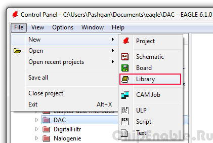
Откроется редактор библиотек. Внешне он похож на редактор схем, только с меньшим количеством инструментов.
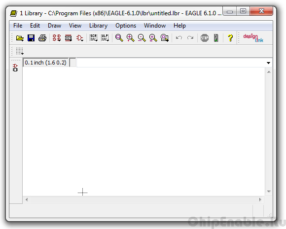
Сразу сохраним нашу библиотеку. Выбираем в верхнем меню File > Save As, указывая папку для сохранения и название библиотеки. Допустим название библиотеки будет test-lib.
Ок. Библиотека создана, но она пока что пустая и не подключена к Eagle`у. Что будет размещаться в библиотеке? Библиотеки обычно содержат три базовых компонента:— Package: посадочное место (футпринт), используемое в редакторе печатных плат
— Symbol: условное графическое обозначение компонента, используемое в редакторе схем
— Device: сам компонент, состоящий из графического символа и посадочного места.Для создания полноценного компонента нам понадобится и посадочное место, и графическое обозначение компонента. Начнем с посадочного места.
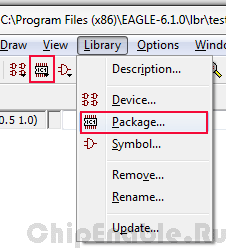
Нажимаем на иконку Package или выбираем в верхнем меню Library > Package.
Откроется диалоговое окно со списком всех посадочных мест библиотеки. Сейчас оно, естественно, пустое. Вводим название нового посадочного места и нажимаем Ок.
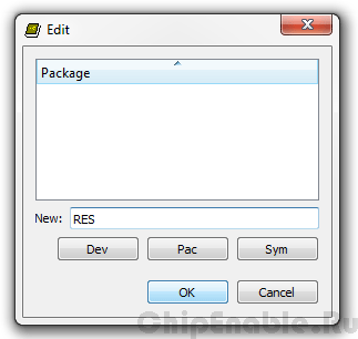
Затем снова Ок, чтобы подтвердить, что мы действительно хотим создать новое посадочное место.
Открылся редактор посадочных мест и для начала мы настроим его сетку. По умолчанию она задается в дюймах (inch), нам нужны миллиметры. Выбираем в верхнем меню View > Grid, откроется диалоговое окно настройки сетки.
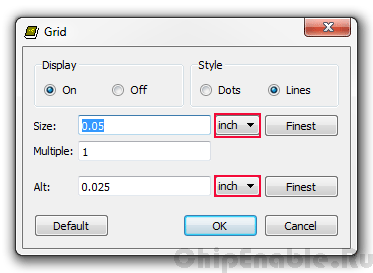
В выпадающих списках выбираем mm вместо inch. Что еще здесь можно настроить?Display — это управление отображением сетки.
Style — стиль отображения сетки: линии или точки.
Size — шаг основной сетки.
Multiple — количество шагов сетки, через которые будут отображаться линии (точки)
Alt — шаг альтернативной сетки. Активируется при нажатии и удерживании кнопки Alt.
Default — установка значений по умолчанию.
Finest — установка наименьшего шага сетки. Настроили сетку, создаем контактные площадки для резистора. Можно создавать площадки для выводных резистора, можно для SMD. У нас первый вариант. Напомню, что большинство действий в Eagle можно выполнить несколькими способами. Например для создания площадки можно нажать на иконку Pad, выбрать в верхнем меню Draw > Pad или набрать в консоли команду pad.
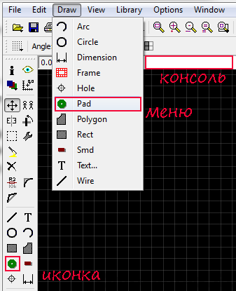
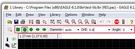
Нажали на иконку Pad. Наверху изменилась панель инструментов и курсор приобрел форму контактной площадки. В панели инструментов можно выбрать форму контактной площадки, внешний диаметр площадки (Diametr), внутренний диаметр отверстия (Drill) и угол поворота площадки (Angle).
Для нашего примера параметры резистора будут такие.
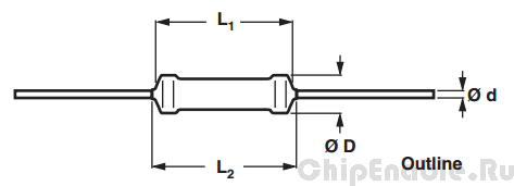
d = 0.58
D = 2.5
L1 = 6.5
L2 = 7.5 Выбираем круглую контактную площадку, внутренний диаметр 0.8 мм нам подойдет, внешний оставим автоматическим. Расставляем две контактные площадки для резистора на рабочее поле редактора. Их нужно поставить симметрично относительно центра, он обозначен белым крестиком. Расстояние, которое должно быть между площадками, нужно выбирать с учетом длины корпуса резистора и расстояний до места изгиба его выводов. Например, можно взять по 3 мм с обоих сторон от корпуса. У меня получилось так.
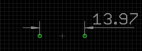
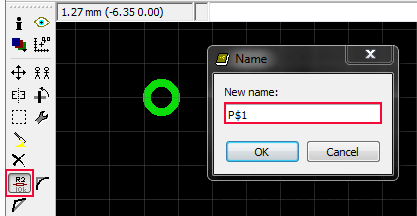
Уже поставленные площадки можно двигать с помощью инструмента Move (меню Edit > Move или кнопка F7). Измерить расстояние между выводами можно с помощью инструмента Dimension (меню Draw > Dimension)Каждая контактная площадка имеет имя. При создании контактной площадки Eagle автоматически присваивает ей имя. Это имя можно изменить с помощью инструмента Name (меню Edit > Name), но для резистора мы не будем этого делать.
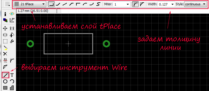
Теперь нам нужно нарисовать обозначение резистора, которое будет использоваться на слое шелкографии при изготовлении печатной платы. Это изображение обозначает место монтажа резистора.Выбираем инструмент Wire (меню Edit > Wire), в верхнем меню выбираем слой tPlace, толщину линии и рисуем. Также в верхнем меню можно менять другие параметры рисования: способ рисования линии (под прямым углом, под углом 45 и т.д.), радиус закругления (miter), тип (непрерывная, пунктирная и т.д.).
На слое tDoc аналогичным образом рисуем более реалистичное изображение резистора. Оно может понадобиться при разводке печатной платы, чтобы располагать компоненты с учетом их реальных размеров или при создании документации. Не будем заморачиваться и нарисуем его в виде прямоугольника чуть большего размера.
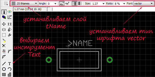
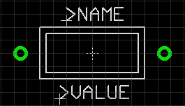
Теперь нужно разместить атрибуты посадочного места — имя и значение. Имя размещается на слое tName. Нажимаем на иконку Text (меню Draw > Text) , вводим в диалоговом окне >NAME, нажимаем Ок. В верхнем меню устанавливаем размер шрифта, векторный тип и размещаем надпись рядом с резистором. Векторный тип шрифта гарантирует нам, что при создании гербер файлов печатной платы надписи никак не изменятся.
Чтобы выйти из режима ввода текста нужно дважды нажать кнопку Esc.Далее повторяем эту процедуру для значения, только размещаем его на слое tValue, а в текстовом поле вводим >VALUE. Сохраняем результат File > save. Посадочное место (футпринт) для компонента готово.
Создание графического обозначения компонента в Eagle
Переходим к созданию условного графического обозначения (УГО) или символа компонента. Выбираем в меню редактора посадочных мест Library > Symbol.
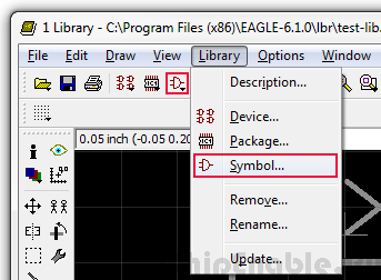
Откроется диалоговое окно со списком всех символов в библиотеке (в нашем случае оно будет пустое), в котором мы должны ввести имя нового символа. После подтверждения намерения создать новый символ, откроется редактор. Настраиваем в редакторе символов шаг сетки. Так же как мы это делали для редактора посадочных мест в меню View > Grid. Теперь нужно нарисовать два вывода. Выбираем инструмент Pin (меню Draw > Pin) и над окном редактора отобразится панель с настройками вывода.
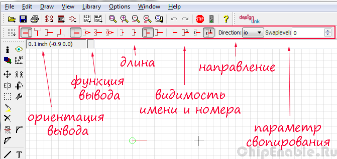
Посмотрим, что это за настройки. Ориентация вывода определяет под каким углом будет расположен наш вывод. Ориентацию можно менять, нажимая на правую кнопку мыши. Функция вывода добавляет к изображению вывода дополнительную графическую информацию — значок инверсии (кружок), тактового входа (треугольник) или оба этих значка.С длиной все понятно.
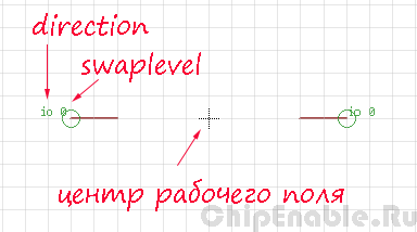
Видимость. У любого вывода есть имя и номер, соответствующий номеру реального вывода. С помощью этой настройки можно задать отображение этих атрибутов. Направление, по сути, определяет назначение вывода — вход, выход, информационный вывод, вывод питания.Параметр свопирования определяет взаимозаменяемость выводов компонента. Свопирование — это операция, используемая при разводке схем. Она позволяет «перекинуть» цепь на другой (идентичный) вывод компонента. Если swaplevel равен 0, то выводы нельзя менять местами. Если больше 0, то выводы с одинаковым swaplevel взаимозаменяемы. Выводы резистора взаимозаменяемы, поэтому для его выводов можно установить этот параметр равным, например, 1. Но поскольку резистор имеет симметричную форму, от этого мы ничего не выиграем. Другое дело микросхемы. Вот там функция свопирования очень помогает. Убираем видимость имени и номера вывода, а остальные параметры оставляем без изменений. Размещаем два вывода на рабочем поле редактора, где-нибудь около центра, который обозначен небольшим крестиком. Когда выводы поставлены, их можно перемещать по рабочему полю с помощью инструмента Move.
Имя вывода можно изменить с помощью инструмента Name, но для резистора нам это не нужно.
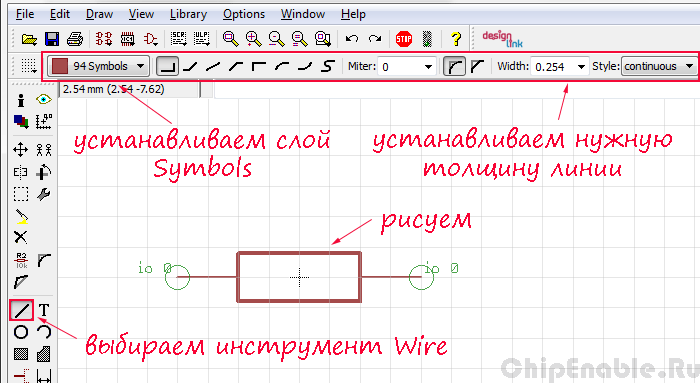
Нарисуем графическое изображение резистора. На отечественных схемах он отображается в виде прямоугольника размером 4 на 10 мм. Нажимаем на инструмент Wire, выбираем слой Symbols, устанавливаем требуемую толщину линии и рисуем. Процесс рисования аналогичен описанному выше. Нарисованный прямоугольник можно двигать с помощью инструмента Move.
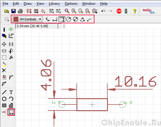
Длину нарисованных линий можно измерять с помощью инструмента Dimension. Нужно его выбрать, кликнуть курсором по начальной точке измерения, по конечной точке и отвести в сторону.
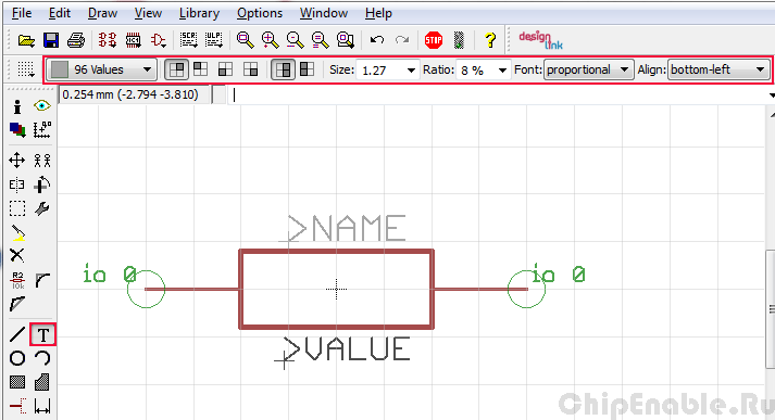
Добавляем символу резистора атрибуты — имя и значение. Выбираем инструмент Text (меню Draw > Text), в открывшееся окно вводим >NAME, устанавливаем слой Names, размер шрифта и размещаем надпись около резистора. Аналогично поступаем и с атрибутом «значение»: текст >VALUE, слой Values. Тип шрифта здесь не важен, можно оставить как есть.
Символ готов, сохраняем полученный результат.
Создание библиотечного компонента в Eagle
Дело за малым — нужно создать компонент, объединив посадочное место и его графическое изображение. Выбираем в меню Library > Device и в открывшемся окне пишем имя нашего нового библиотечного компонента. Откроется очередной редактор.Вызываем инструмент ADD (меню Edit >Add) и добавляем на рабочее поле символ резистора.
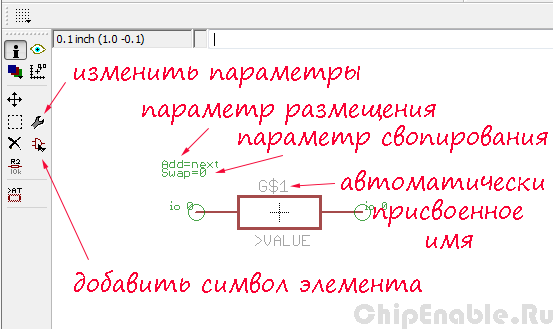
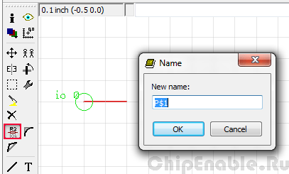
У появившегося изображения есть два параметра. Addlevel — параметр размещения. Определяет характер размещения компонентов, он имеет значение для элементов состоящих из нескольких частей или блоков (как, например, логические микросхемы), поэтому мы рассмотрим его в следующий раз. Swaplevel — параметр свопирования. О нем я уже упоминал выше, только в данном случае этот параметр относится не к выводам компонента, а к его частям. У нас никаких блоков нет, поэтому его тоже пропустим. G$1 — это автоматически присвоенное имя. Чтобы резистор именовался на схемах с буквой R, нужно вписать ее в поле Prefix.
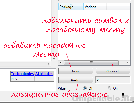
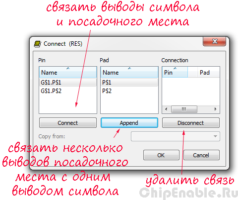
С правой стороны нажимаем кнопку New и добавляем компоненту посадочное место. Затем нажимаем Connect и связываем выводы символа с выводами посадочного места.
С помощью кнопки Append можно связывать несколько выводов посадочного места с одним выводом символа. Сохраняем результат. Компонент готов!Подключить его к проекту можно из редактора схем с помощью меню Library > Use.
Продолжение следует…
Ссылки
Eagle Cad. Рисование схемы